vyktormvmpay25
Senior Member
I'm sorry, we tried, I say I can't do much more as didn't discover myself at right time.
I don't see were else could be.


I don't see were else could be.
Thank you for your help, so I solder wires from 3.3V to MB RX and from 0.75V to MB TX(or opposite) and leave my wires connected to mb points as before, plug power and then do I write something to the syscon or open putty first? A bit confused about that part, sorry. Also did I mess something up by sendingI'm sorry, we tried, I say I can't do much more as didn't discover myself at right time.
I don't see were else could be.
EEP SET 3961 01 00

Thank you for your help, so I solder wires from 3.3V to MB RX and from 0.75V to MB TX(or opposite) and leave my wires connected to mb points as before, plug power and then do I write something to the syscon or open putty first? A bit confused about that part, sorry. Also did I mess something up by sendingCode:EEP SET 3961 01 00
EEP GET 3961 01I actually tried that and got back FFFFA501Look at this table as reference (and click in the arrow at top for "sherwood" to reorder the table rows)
https://www.psdevwiki.com/ps3/Talk:SC_EEPROM#Experimental_table
It seems offset 0x3961 is out of the "rewritable" areas... so probably you didnt wrote anything
For a confirmation try to do the inverse process, you tryed to write byte 00 at offset 0x3961... so try to read it and see if is different than 00
If the result is different than 00 it means you didnt wrote anything, most probably is not going to show anything because as i said you are trying to read/write in protected areas where there is no read/write accessCode:EEP GET 3961 01
Sir if you see the pictures i shared above in post from your pictures i measured 0.75V and 3.3V points. I just want some guidance specifics on what to do with these pins, (solder them to normal rx tx pins and then write command "w 1202 02" and then open putty? thank you for your help.In SW models you aren't able to read anything over 1400h. 13ff limited on uart.
So don't worry I will share those SB pins with time whenever I get same board here.
You have a glod issue, if you consider rsx is good by checking all measurements try reball same , or exchange.
Hello, what do you mean you're not confident to test yourself? I soldered to the top 3v3 point and 0.75 to the right of the two pads, swapped rx and tx a couple of times to no avail,if you had a board how would you go about finding the sb rx tx? I'm dedicated to finding them unless it's a putty fault, I use default settings speed 9600 nothing shows up on putty :/. I have written 1202 02.We connect on normal uart on syscon SW ic and we write that address 1202 02. After if we know what second uart port is for SB(southbridge ic) we connect to that uart port (rxtx). At this point I'm afraid I can't help anymore for this board as I am not confident to test myself.
It suppose to show automatically log when we open putty software with uart adaptor soldered to second uart port for SB.
Read and watch over this thread examples I've posted back.
Uart port for SB is always accessible only when unit it can stay open as glod mode.

 Should i gave up on these? Seller said he heated both mobos with heat gun so he could be completely burned the cpu maybe or damaged the layers of the board? because it has terrible swelling on middle of the board. I changed %50 of nec tokins by the way in case if its that.
 So IDK where u got the idea to solder to that 3.3v pad, but all you need to do is connect 2x wires to the outter most pads on the pci port. Like in the example image I posted before. Did that not work or something?Hello, what do you mean you're not confident to test yourself? I soldered to the top 3v3 point and 0.75 to the right of the two pads, swapped rx and tx a couple of times to no avail,if you had a board how would you go about finding the sb rx tx? I'm dedicated to finding them unless it's a putty fault, I use default settings speed 9600 nothing shows up on putty :/. I have written 1202 02.
Yes the system gets that far and I have sent the write command and confirmed with read, this is the hookup(while testing I only had right wire soldered to pad so no chance of shorting) and sadly pulled the pad because jumper wire a bit too big and heavy and wasn't as careful when trying to pass it through the shield.So IDK where u got the idea to solder to that 3.3v pad, but all you need to do is connect 2x wires to the outter most pads on the pci port. Like in the example image I posted before. Did that not work or something?
Victor's just saying you first have to enable the SB UART bit in SYSCON UART before switching over to the SB UART. And that the SB log wont start until the bootloader does. So the console needs to be able to get at least that far into the booting process or it wont start logging anything.
Please post a picture of how you hooked the wires up.


Wait, do you mean I should bridge them? What is that equal symbol there? Thank you.I'm sorry, we tried, I say I can't do much more as didn't discover myself at right time.
I don't see were else could be.


Ok so at this stage you got it right this I'm often calling myself "special glod". If reball or exchange of this rsx not going to change its working status I suggest recap totally 12x470uF caps on both, use vdd for core minimum total wire 3mm diameter.Wait, do you mean I should bridge them? What is that equal symbol there? Thank you.
EDIT:Nevermind, here you go sir. It was the 2 round points you had circled here. Pay NO attention to the fataldown start error, I had not plugged psu cable all the way in.
Boot Loader SE Version 4.8.6 (Build ID: 5353,50715, Build Date: 2020-01-30_ 11:23:58)
SDK Version: 486.000
Copyright(C) 2020 Sony Computer Entertainment Inc.All Rights Reserved.
[INFO]: === eXtreme Data Rate Memory Subsystem ===
[INFO]: (Configured Memory Size per single XIO channel: 128 MBytes.)
[INFO]: XIO channel[0] is available.
[INFO]: XIO channel[1] is available.
[INFO]: ---> Total 256 MBytes are now in use.
[INFO]: SPU enable [0, 1, 2, 5, 6, 7] 11101111
[INFO]: BE:11S DD1.0, SB:SX1.2
Cell OS SDK4.8.6 000 (release build: r50715 2020_01_30_110000)
Copyright 2020 Sony Computer Entertainment Inc.
revision: 50702
date: Thu Jan 30 11:25:44 JST 2020
skip 2nd initialization step
lv2(0): total memory size: 249MB+640KB
lv2(0): kern memory size: 12MB+640KB (heap:3492KB page pool:4736KB)
lv2(0): user memory size: 237MB
lv2(2):
lv2(2): Cell OS Lv-2 32 bit version 4.8.6
lv2(2): Copyright 2011 Sony Computer Entertainment Inc.
lv2(2): All Rights Reserved.
lv2(2):
lv2(2): revision: 50715
lv2(2): build date: 2020/01/30 11:30:24
lv2(2): processor: Broadband Engine Ver 0x0000 Rev 0x1000
lv2(2): PPU:0, Thread:0 is enabled.
lv2(2): PPU:0, Thread:1 is enabled.
lv2(2): rsx: rsx65 a06 500/650 vpe:ff shd:6f [AP0011327:1:1:a:b:13:2:5:1][ 3d:0:2:0:1:2:0][2:1:0]
lv2(2): Available physical SPUs: 6/7
lv2(2): mounting the flash file system : ........... Failed (error code:0x800100 2b)
lv2(2):
lv2(2): ###
lv2(2): ### Safe mode
lv2(2): ###
lv2(2):
lv2(2): creating the recover process (for safe mode) : OK
lv2(2): sys_storage_get_device_info() failed. 0x80010002.
lv2(2): RescueUtilityGetStorageCapacity() failed. 0x1.
lv2(2): this system has no available hard disk.
lv2(2): please attach hard disk drive.Boot Loader SE Version 4.8.6 (Build ID: 5353,50715, Build Date: 2020 -01-30_11:23:58)
SDK Version: 486.000
Copyright(C) 2020 Sony Computer Entertainment Inc.All Rights Reserved.
[INFO]: === eXtreme Data Rate Memory Subsystem ===
[INFO]: (Configured Memory Size per single XIO channel: 128 MBytes.)
[INFO]: XIO channel[0] is available.
[INFO]: XIO channel[1] is available.
[INFO]: ---> Total 256 MBytes are now in use.
[INFO]: SPU enable [0, 1, 2, 5, 6, 7] 11101111
[INFO]: BE:11S DD1.0, SB:SX1.2
Cell OS SDK4.8.6 000 (release build: r50715 2020_01_30_110000)
Copyright 2020 Sony Computer Entertainment Inc.
revision: 50702
date: Thu Jan 30 11:25:44 JST 2020
skip 2nd initialization step
lv2(0): total memory size: 249MB+640KB
lv2(0): kern memory size: 12MB+640KB (heap:3492KB page pool:4736KB)
lv2(0): user memory size: 237MB
lv2(2):
lv2(2): Cell OS Lv-2 32 bit version 4.8.6
lv2(2): Copyright 2011 Sony Computer Entertainment Inc.
lv2(2): All Rights Reserved.
lv2(2):
lv2(2): revision: 50715
lv2(2): build date: 2020/01/30 11:30:24
lv2(2): processor: Broadband Engine Ver 0x0000 Rev 0x1000
lv2(2): PPU:0, Thread:0 is enabled.
lv2(2): PPU:0, Thread:1 is enabled.
lv2(2): rsx: rsx65 a06 500/650 vpe:ff shd:6f [AP0011327:1:1:a:b:13:2:5:1][ 3d:0:2:0:1:2:0][2:1:0]
lv2(2): Available physical SPUs: 6/7
lv2(2): mounting the flash file system : ........... Failed (error code:0x800100 2b)
lv2(2):
lv2(2): ###
lv2(2): ### Safe mode
lv2(2): ###
lv2(2):
lv2(2): creating the recover process (for safe mode) : OK
Wait, do you mean I should bridge them? What is that equal symbol there? Thank you.
EDIT:Nevermind, here you go sir. It was the 2 round points you had circled here. Pay NO attention to the fataldown start error, I had not plugged psu cable all the way in.
Boot Loader SE Version 4.8.6 (Build ID: 5353,50715, Build Date: 2020-01-30_ 11:23:58)
SDK Version: 486.000
Copyright(C) 2020 Sony Computer Entertainment Inc.All Rights Reserved.
[INFO]: === eXtreme Data Rate Memory Subsystem ===
[INFO]: (Configured Memory Size per single XIO channel: 128 MBytes.)
[INFO]: XIO channel[0] is available.
[INFO]: XIO channel[1] is available.
[INFO]: ---> Total 256 MBytes are now in use.
[INFO]: SPU enable [0, 1, 2, 5, 6, 7] 11101111
[INFO]: BE:11S DD1.0, SB:SX1.2
Cell OS SDK4.8.6 000 (release build: r50715 2020_01_30_110000)
Copyright 2020 Sony Computer Entertainment Inc.
revision: 50702
date: Thu Jan 30 11:25:44 JST 2020
skip 2nd initialization step
lv2(0): total memory size: 249MB+640KB
lv2(0): kern memory size: 12MB+640KB (heap:3492KB page pool:4736KB)
lv2(0): user memory size: 237MB
lv2(2):
lv2(2): Cell OS Lv-2 32 bit version 4.8.6
lv2(2): Copyright 2011 Sony Computer Entertainment Inc.
lv2(2): All Rights Reserved.
lv2(2):
lv2(2): revision: 50715
lv2(2): build date: 2020/01/30 11:30:24
lv2(2): processor: Broadband Engine Ver 0x0000 Rev 0x1000
lv2(2): PPU:0, Thread:0 is enabled.
lv2(2): PPU:0, Thread:1 is enabled.
lv2(2): rsx: rsx65 a06 500/650 vpe:ff shd:6f [AP0011327:1:1:a:b:13:2:5:1][ 3d:0:2:0:1:2:0][2:1:0]
lv2(2): Available physical SPUs: 6/7
lv2(2): mounting the flash file system : ........... Failed (error code:0x800100 2b)
lv2(2):
lv2(2): ###
lv2(2): ### Safe mode
lv2(2): ###
lv2(2):
lv2(2): creating the recover process (for safe mode) : OK
lv2(2): sys_storage_get_device_info() failed. 0x80010002.
lv2(2): RescueUtilityGetStorageCapacity() failed. 0x1.
lv2(2): this system has no available hard disk.
lv2(2): please attach hard disk drive.Boot Loader SE Version 4.8.6 (Build ID: 5353,50715, Build Date: 2020 -01-30_11:23:58)
SDK Version: 486.000
Copyright(C) 2020 Sony Computer Entertainment Inc.All Rights Reserved.
[INFO]: === eXtreme Data Rate Memory Subsystem ===
[INFO]: (Configured Memory Size per single XIO channel: 128 MBytes.)
[INFO]: XIO channel[0] is available.
[INFO]: XIO channel[1] is available.
[INFO]: ---> Total 256 MBytes are now in use.
[INFO]: SPU enable [0, 1, 2, 5, 6, 7] 11101111
[INFO]: BE:11S DD1.0, SB:SX1.2
Cell OS SDK4.8.6 000 (release build: r50715 2020_01_30_110000)
Copyright 2020 Sony Computer Entertainment Inc.
revision: 50702
date: Thu Jan 30 11:25:44 JST 2020
skip 2nd initialization step
lv2(0): total memory size: 249MB+640KB
lv2(0): kern memory size: 12MB+640KB (heap:3492KB page pool:4736KB)
lv2(0): user memory size: 237MB
lv2(2):
lv2(2): Cell OS Lv-2 32 bit version 4.8.6
lv2(2): Copyright 2011 Sony Computer Entertainment Inc.
lv2(2): All Rights Reserved.
lv2(2):
lv2(2): revision: 50715
lv2(2): build date: 2020/01/30 11:30:24
lv2(2): processor: Broadband Engine Ver 0x0000 Rev 0x1000
lv2(2): PPU:0, Thread:0 is enabled.
lv2(2): PPU:0, Thread:1 is enabled.
lv2(2): rsx: rsx65 a06 500/650 vpe:ff shd:6f [AP0011327:1:1:a:b:13:2:5:1][ 3d:0:2:0:1:2:0][2:1:0]
lv2(2): Available physical SPUs: 6/7
lv2(2): mounting the flash file system : ........... Failed (error code:0x800100 2b)
lv2(2):
lv2(2): ###
lv2(2): ### Safe mode
lv2(2): ###
lv2(2):
lv2(2): creating the recover process (for safe mode) : OK
@vyktormvmpay25 in your "special GLOD" (as you call it), Is it normal that it complains about not being able to mount the flash system?Ok so at this stage you got it right this I'm often calling myself "special glod". If reball or exchange of this rsx not going to change its working status I suggest recap totally 12x470uF caps on both, use vdd for core minimum total wire 3mm diameter.
In case is a board issue and rsx good, it should remain in this stage of glod.
I've pointed those small bridges (=) as those will be used in case you want to pass those together to a side unsoldered port like having all grouped in one port.
Usually for me only exchange rsx was working.
I also think I killed some 40nm while deliding ihs. Well on 65nm delid should be easy but not necessarily reball process won't kill in some way ic from heat.
So I know on all my test all boards should stay in same condition, not worst.
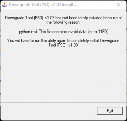
Cool, I'll upload directly here, I do have an E3 Nor flasher, not much use for this specific console, also bought teensy 2++ from aliexpress but even though I have soldered 3v3 regulator on it and soldered 3v3 pads together and seperared 5v, light on it doesn't come on(comes if no reg is on and 5v are connected together) also the downgrade tool 1.03 gives me a python msi invalid data error(running windows 11). A bit random, just because you said it may be nand nor issue thought maybe i'd bring it up. Thank you both for all your help so far.@vyktormvmpay25 in your "special GLOD" (as you call it), Is it normal that it complains about not being able to mount the flash system?
Because that sounds like a NAND/NOR or StarShip2 issue. Maybe he should inspect the pins on the flash to be sure they are connected correctly. Or perhaps they got corrupted?
BTW: @Kostaslgr7 you should be able to attache pics direct to the forum now since you have over 10 posts. Will make life easier for you.