DoublesAdvocate
Member
I wonder if they might just be installing them on the underside of the motherboard to avoid any signal integrity issues from running the wires near large capacitors, coils, etc.Im tempted to try to compare the images availables to try to figure which wire is each by his name (the 3 from the SPI bus). The best thing we could do with that info is to take the images posted by @DoublesAdvocate and paint on top of them the SPI names of each wire
This could help a bit if someone is interested to "sniff" the SPI communications
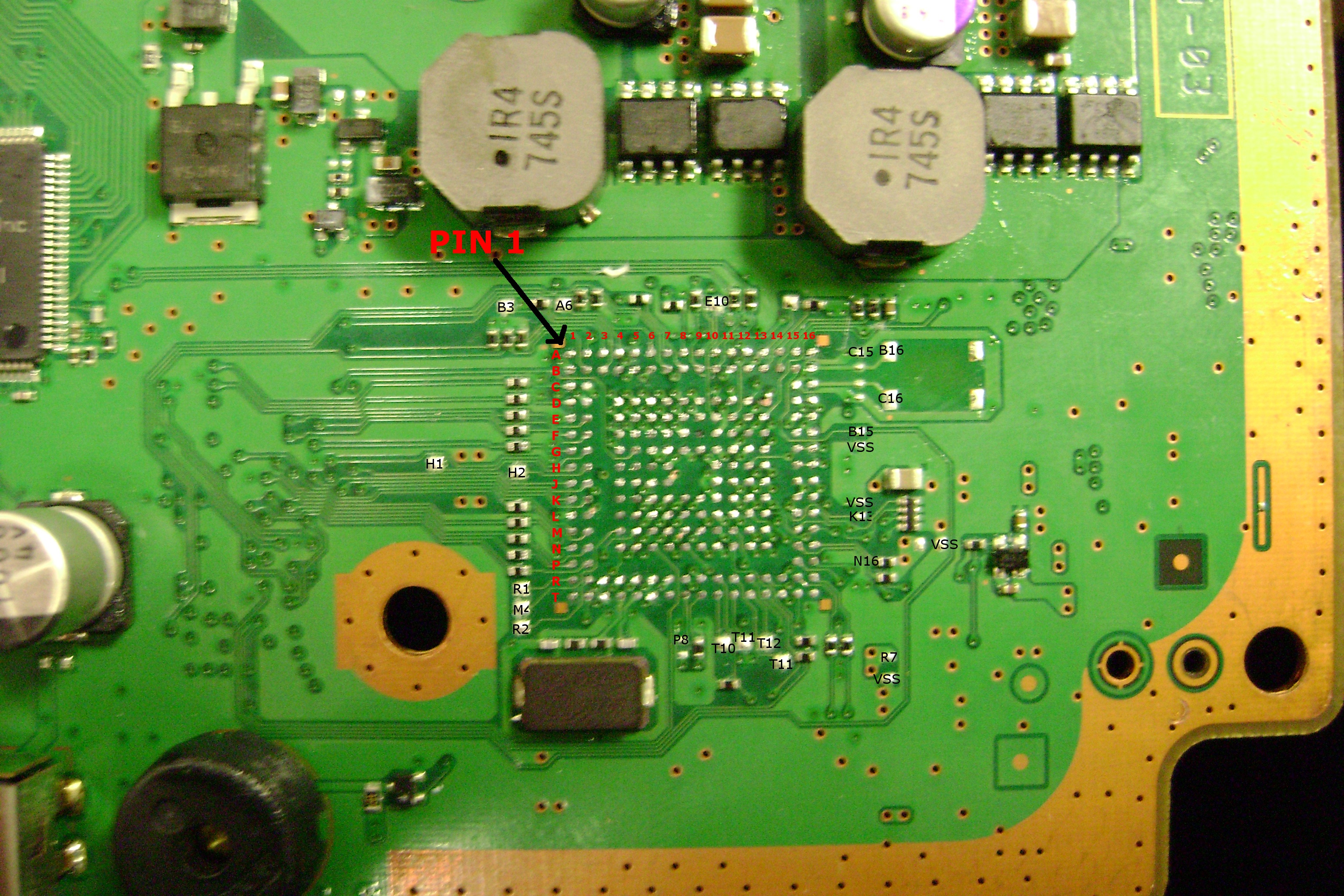
In wiki there is a photo of a DIA-001 with the syscon removed... is a bit blurry, but i guess this one is good enought
It allows to see where is located each solder pad, we can see where the trace goes to a "via" (hole) and allows to follow it with a multimeter... it should match with the photos of the modchip installations
I noticed the photos of the modchip instalaltions are always soldered to vias... and at an intermediate point of some kind of bigger "data bus"... so most probably the modchip can be installed in any side of the motherboard, keep that in mind because we are not restricted to do the connections exactly like in the photos of the modchip installations
I mean... for every photo of the modchip installation... we can consider there are "alternative" solder points at the other side of the motherboard
")
Hopefully those chips should arrive soon and we'll be able to find out exactly which ones they are and also get some better scans of the installation methods.


")
.jpg")