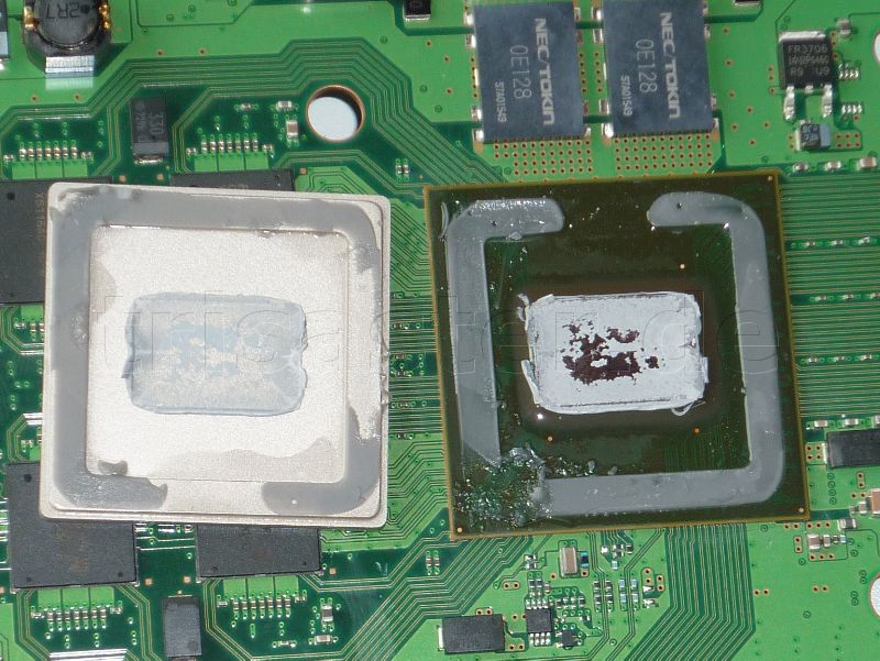
the support bracket surely will help the solderballs under to kept good. but gpus back then ~2005-2008 give or take. had premature fail. and the reason most of the times was the solderbals between dye and substrate. i had a launch xbox 360 it fails with rrod within a year. but my 2010 xbox jasper is still strong. heres a video explaining the issue. but again there are gpu fails with problem in main pcb and substrate crack solderbals. so in this case puting LM and secure back the ihs would be the perfect repair. i said LM because is not dryed out over time like thermal paste
View attachment 35615
Has it escaped anyone else's attention that the PS4/5 APU has a support bracket around the edge of the interposer?
What do we know about the PS3? Oh yeah, it had issues with the YLOD! Hmm...
I just want to point out that the edges of the chip is where we are seeing the most BGA defects (FlexIO and VDDIO errors). Perhaps the purpose of this bracket (which add cost to the BOM BTW) is to provide support to the solderballs underneath.
Is also intended to prevent cracking the corners/edges of the DIE. I still have a old AMD athlon from a friend with that problem, it happened because he was mounting the heatsink incorrectly or/and he was rotating the heatsink when he was assembling or dissasembling it
Under microscope it can be seen the DIE have a "fracture line" all along and a couple of corners broken like an stone. The funny thing is that it still works, allows to install an OS, but is very unestable, it seems it have some of the internal circuitry broken, lol
I guess this is the main reason why later the manufacturers was using a IHS, is to prevent us to break the DIE, for a company as sony it also helps his tecnicians in the repair service to dont fall in this problem too
If you ask me... i dont like that solution, is like a restriction because they was assuming we are dumbs
The metal bracket used nowadays is a lot better solution for that matter because also prevents us breaking the DIE.. you know... is a matter of geometry, if we rotate the heatsink while is attached all the pressure/force is going to be concentrated at the edge of the bracket (not the edge of the DIE) so nothing breaks
----------
For the matter of spreading the pressure to the edges of the substrate there is a very important detail that worths to be mentioned, is again a problem of geometry and is not so easy to solve
Think in the PS3 RSX, it have a DIE at the center and 4 VRAM chips at the corners... then the IHS is "glued" on top of them, right ?
Well... the problem here is we have a single surface (the IHS) that is going to touch with other 5 surfaces (DIE and VRAM chips)... so the 5 surfaces should have exactly the same height (with a huge precission of micrometers)
But the manufacturing processes doesnt allows to adjusts 5 surfaces of 5 different "components" to an identical height... so what they did in the PS3 RSX was to give the DIE a higher height than the VRAM chips
The result is we only have one surface (the IHS) touching with other surface (the DIE)... and the 4 VRAM chips are not really touching the IHS (there is a "gap" in them), we fill that gap with thermal glue that have a bigger density than the standard thermal paste, and is intended to solidify and fill gaps
----------
So... the metal brackets used nowadays are nice in concept, but everything depends of how they are "aligning" his height with the height of the DIE at the center
If the metal bracket have a higher height than the DIE then the pressure would be concentrated all along the bracket, but the center DIE will not have any pressure (a little gap of micrometers could have a critical impact in thermal performance)
I dont think they can align the heights of the DIE and the metal bracket with a precission of micrometers, most probably they are "playing safe" giving the bracket a height smaller than the DIE and glueing with epoxy
Or... the bracket is glued with a silicone that is flexible to allow it to adjust his height. I mean... the silicone have the density of the rubber, it can be compressed, so the height of the metal bracket is variable
Good point. And the thermal adhesive is yet another material with a different CTE (Coefficient of Thermal Expansion). So we have, a Copper IHS, resin memory module, its lead-free solder balls and underfill, a Silicon DIE and its lead-free bumps and underfill, the FR4 interposer and it's lead-free solderballs. Not to mention all the SMDs on the RSX too! All of these different materials factor into stresses and forces placed on their connection.
There is too much complexity. It violates the adage, "keep it simple, stupid!"
View attachment 35615
Has it escaped anyone else's attention that the PS4/5 APU has a support bracket around the edge of the interposer?
What do we know about the PS3? Oh yeah, it had issues with the YLOD! Hmm...
I just want to point out that the edges of the chip is where we are seeing the most BGA defects (FlexIO and VDDIO errors). Perhaps the purpose of this bracket (which add cost to the BOM BTW) is to provide support to the solderballs underneath.
Effectively there are 2 problems that cause YLOD:
Bump failures = reduced to acceptable levels with better underfill and cooling. Perhaps by abandoning the diamond pattern that could cause tortional stresses as the interposer twists from the geometry mismatch.
BGA failures = reduced with interposer support bracket, better soldering process, and better cooling.
The CPU IHS has a ring and is silconed around the edge, effectively providing support.
This brings up a serious oversight and concern about delidding! We really should be gluing the IHS back on after repasting. Both the RSX and CPU IHS! With that in mind, then it changes the TIC decision for me immensely! I think a graphite thermal pad is the way to go. It can be taped (kapton) to the IHS so it never moves out of position and shorts anything out. It prevents die hot spots by transferring thermals laterally extremely fast. And it never degrades. It will perform the same forever, so the IHS can be glued down and never delidded again. You may even be able to silicone the RSX IHS down, to provide extra support for the interposer. Perhaps that wiould make the RSX more reliable. The downside is that graphite thermal pads don't transfer heat to the IHS as well as high quality pastes do. They're a few C worse. Not bad, mind you! They are still good, just not great.
I'd say this has more to do with AMD being the manufacturer of these APUs, AMD has been making them with those metal "shields" for ages now when it comes to BGA soldered APUs. They may or may not help prevent YLOD, I can't argue about that because I don't have proof for either case, but it's been AMD's standard for quite a while.
I'd say this has more to do with AMD being the manufacturer of these APUs, AMD has been making them with those metal "shields" for ages now when it comes to BGA soldered APUs. They may or may not help prevent YLOD, I can't argue about that because I don't have proof for either case, but it's been AMD's standard for quite a while.
Yep, is something decided by AMD, and i guess they will keep doing it in his APUs for some more time because all them are "monolithic" (CPU, GPU, IO and many other controllers in the same piece of silicon), the manufacturing process is more expensive than other desktop CPUs that have several DIEs, but is very convenient for thermal performance and other reasons
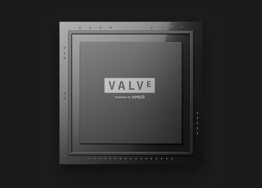
That design is pretty cool imo, but when the valve steam deck was announced they published a photo that disturbed me a bit
I dont understand if this is a render of a conceptual design but is a bit awesome, it have that "bracket" all around that seems to be made of the same material than the square at the center... and everything seems to be made with huge precission and looks very "solid"
Im mentioning this because the APU of the steam deck is an old AMD design... whatever technology they used in it is ready to be deployed in other APU models... so it would not surprise me if at some point we see this new packaging style, it looks really nice in that photo
Yesterday I made a post about the YLOD and the role BGA/Bumps play in it. I will edit it over time to improve it, but I just added some useful information about the bracket.
I just found what it's called and did some research into it. It's called a window stiffened FCBGA package. There are other strategies to stiffen the interposer and prevent package warpage too. I edited the post to include it. Check it out.
Having read this, I am now convinced it is a REALLY bad idea to delid and not glue the IHS back on! We are hastening a BGA failure doing that!
the metal bracket the ps4 xbox one and their successors has on the apu surrely secure things. but there is something else too here xbox 360 phat consoles have the heatsink touching the diy, the cpu have a diy in the center, the gpu have a diy in the center and a diy direct above the main diy (edram) yet any phat console manufacture before 2008 will have rrod and the cause is the gpu. cpu issues are rare like ps3. but both gpus and cpus never had a design change, newer simply are smaler in nm. the ps3 in the other hand has more secure gpu according to what you say. a diy in the center and four ram chips one in each corner yet the 90nm are suffer from premature failure. while 65nm and 40nm whitch is same design last way longer. so smaller in nm plays a role for durability too.
Yep, is something decided by AMD, and i guess they will keep doing it in his APUs for some more time because all them are "monolithic" (CPU, GPU, IO and many other controllers in the same piece of silicon), the manufacturing process is more expensive than other desktop CPUs that have several DIEs, but is very convenient for thermal performance and other reasons
That design is pretty cool imo, but when the valve steam deck was announced they published a photo that disturbed me a bit
I dont understand if this is a render of a conceptual design but is a bit awesome, it have that "bracket" all around that seems to be made of the same material than the square at the center... and everything seems to be made with huge precission and looks very "solid"
Im mentioning this because the APU of the steam deck is an old AMD design... whatever technology they used in it is ready to be deployed in other APU models... so it would not surprise me if at some point we see this new packaging style, it looks really nice in that photo
I'd say it's a conceptual render, it just looks to good to be functional lol, also the seemingly matte finish of the die is either a resin covered die or just a conceptual render made to look good, and I don't think they're gonna cover the die with resin so probably just a cool concept. We'll have to wait and see
...newer simply are smaler in nm. the ps3 in the other hand has more secure gpu according to what you say. a diy in the center and four ram chips one in each corner yet the 90nm are suffer from premature failure. while 65nm and 40nm whitch is same design last way longer. so smaller in nm plays a role for durability too.
Yes. Later model PS3/360's are more reliable, despite the fact the chip design changed very little (aesthetically), because they reduced the the temperature Delta. Smaller manufacturing process allowed them to pack the same performance into a more power efficient die. So less heat to sink and less warpage. Also the fan curves were adjusted, fans themselves were changed, different heatsinks, the airflow in the case was redirected, the method of attaching the IHS was changed, etc. Basically, they improved the thermal design over successive model iterations to improve reliability to an acceptable level while lowering BOM costs.
All of this started because SONY and Microsoft were chasing graphics. They wanted the most powerful hardware and it bit them in the cheek (whichever one the keep their wallet). Nintendo on the other hand chose to stay out of that arena. That's why their consoles avoided getting caught up in this. Basically, the solder joints couldn't take the heat using the same old design principals. Reliability suffered. It's not like the demand for hot chips that push BGA technology to the reliability limit has gone away. Just look at the RTX family of GPU's. You can't even overpay for them! That's why they had to come up with a strategy to improve reliability to an acceptable level. What is an "acceptable" level of reliability? 10 years? It depends on your perspective. Well, SONY's, not ours (gamers/customers)! They only care about our perspective of reliability in so far as we keep buying their product. So it just can't fail in the first few years, leaving a bad impression or getting them sued.
Regardless, chip designers added the stiffener in subsequent hot chips. It serves 2 purposes. First, heatsinks can interface directly with the die, instead of having the IHS and a second TIM in the way. That increased thermal transfer efficiency. Second, it physically braces the interposer keeping it from flexing. It probably also helps keep the DIE from cracking from uneven force applied when seating down the heatsink, as @sandungas pointed out. Another strategy is to flood the area around the die with resin.
The strat is to use materials with the smallest difference in CTE and then Stiffen the shiz out everything. All to avoid using a socket.
The whole industry was forced to do a better job of modeling the stresses and thermal design. They had to revamp their testing procedures, quality assurance and warranty repairs. Bumpgate woke the industry up! But they just worked around it. They still refuse to put a socket in!
Here's the conspiracy theory part. They don't want you to be able to upgrade/repair your game console. They want it to break so they don't have to compete with it. About 10 years seems to be the console cycle. After that, they want you to migrate to their new console and buy games they make a profit on. They don't want you to be satisfied buying used games from a market they don't profit on. It competes against them. And that's why they are employing digital only, DLC, broken games on disc. They want to destroy the used games market and control the retro gaming scene. They want to funnel us all (modern and retro gamers) into a subscription service for that experience. Subscriptions are the holy grail of business. All digital cuts out the logistical nightmare and expense. No more negotiating prices with factories that press the disc, transportation companies who ship them, or retailers who stock/sell them. None of that! Direct to consumer! Larger margin, reliable, projectable profits! Exactly the type of thing investors want to see. Guaranteed income and growth potential.
Yesterday I made a post about the YLOD and the role BGA/Bumps play in it. I will edit it over time to improve it, but I just added some useful information about the bracket.
I just found what it's called and did some research into it. It's called a window stiffened FCBGA package. There are other strategies to stiffen the interposer and prevent package warpage too. I edited the post to include it. Check it out.
Having read this, I am now convinced it is a REALLY bad idea to delid and not glue the IHS back on! We are hastening a BGA failure doing that!
Have you noticed in the image (at most left) you posted they are drawing the height of the stiffen a bit smaller than the height of the DIE ?
This is what i meant when i said most probably they are "playing safe"... because this way assures the DIE and the heatsink surfaces are going to have a good contact with each other
But the flaw of it is by doing that we are transfering 100% of the pressure to the DIE (and nothing to the stiffen)... so the stiffen is not increasing the structural resistance at the borders so much
This kind of adjustments of heights in between the DIE and the stiffen is not so easy to achieve, at least industrially, maybe they have some machines messuring distances with lasers etc... but still is very hard to do it with huge preccision
The industry is still trapped in that problem
The only way i see to do it with huge precission is if you assemble everything, and at the last step of the production you do some kind of "lapping" to the combined surfaces (DIE and stifffen lapped together)
The APU from the steam deck looks a bit like that, as @blckbear_ said it looks like some kind of resine... or maybe they are using some other material that is "fused" with the silicon of the DIE ?... dunno, but im eager to see the final product to see if they nailed it or it was just a wet dream
...The only way i see to do it with huge precission is if you assemble everything, and at the last step of the production you do some kind of "lapping" to the combined surfaces (DIE and stifffen lapped together)
The APU from the steam deck looks a bit like that, as @blckbear_ said it looks like some kind of resine... or maybe they are using some other material that is "fused" with the silicon of the DIE ?... dunno, but im eager to see the final product to see if they nailed it or it was just a wet dream
Yeah, I was wondering if we could find out the exact resin material used to make FCmBGA and use it to mold around a delidded RSX. Then lap it down to the RAM modules. But since the DIE is lower, we'd need to mask/shim the die. Then we could use a copper shim for the IHS.
I abandoned the idea because it seems too difficult to achieve. On the other hand it wouldn't be too hard to redesign the IHS with L support for areas between the SMDs. Then we can use thermal adhesive on RAM modules + Silicone on the parts that stiffen the interposer. A graphite thermal pad would never degrade or loose performance (even though it's slight worse than high quality TIM). It's still great TIM, and we would need something that cannot go bad locking everything together like this.
Hmmm, is a bit extreme but i like it, lets use CELL for this example (after desoldering it from the mothrboard) just because is easyer than RSX
We can create a container "box" all around... with 4 pieces of plastic located vertically all around the borders
We place it in a flat surface because we are going to drop "liquid" inside the box
Then we drop a lot ot resin in the box. An excess of resin, even covering the DIE a bit because is going to reduce its volume when drying
After that we can do a lapping to expose the DIE... in other words... we are lapping the resine, not the DIE
This would result in a solid squared piece with the same thickness everywhere, structurally very solid, it could handle lot of pressure and that pressure should be spreaded evenly
As said... this is a bit extreme because everything where is involved epoxy resines is a "one way procedure"... you know there is no way to step back because is almost imposible to remove the epoxy without causing damages, if something goes wrong is a game over
That would work for the CPU, but it's not really necessary. The IHS is already designed well enough. It's the RSX that's problematic.
I wonder how far into the ram moduls you can lap before exposing something critical? If you can lap away enough to get to the RSX DIE without ruining the RAM modules first, that could work.
I remember vyktor was doing some experiments by replacing the RSX ram chips from some dead RSX's, just to see if the problem was in the solders under the ram chips, and also to see how tricky is to reball the ram chips
I guess most of the ram chips involved in that experiments are still working fine but maybe he have one fryed to check what you said (a decapping)
Meassure the original thickness, then start sandpapering it to expose the circuitry inside it and measure the thickness again
I'm not super interested to try it, but I have 3 or 4 delidded RSX from failed reballs lying around. It's a simple matter of sanding them down to the die and seeing if anything important is exposed in the ram modules, or if it's all resin till you get to the die. Probably depends on the specifi ram module though. If I remember correctly there are 2 or 3 different ones used, depending on model. Maybe even between the same model.
I like the idea of designing a new IHS better. There are companies that sell custom milled parts like this at reasonable prices. Just need to brace a few spots. Specifically the gap above the FlexIO where people are inserting their prying tool for delidding (that must not be good for the balls under there BTW).
The other 3 parts have SMDs in the way. I'm not sure there's any way to brace there. But there's a little room around the die for some bracing. There is also a very small lip around the edge that if the custom IHS were designed and milled with precision could be used to help brace all the way around.
PM me, I'm still working on this. Some of the information is in flux. I just want to make sure what you mention is accurate, at least as far as I understand it.
Btw apparently, you can most likely get the modchip to work on refurbished boards as well. Obviously, it would only make sense if you plan to install a 40nm on refirbished boards with a 65nm that use 303GB syscons (which won't support 40nm). You must bridge different pads, just like you would for the slim boards.
At least for the moment it was tested by @vyktormvmpay25 on dia002. Somebody should test this on a refurbished cok as well.
I've also copied the orbis service pictures that our friend has shared into this video.
Has anybody tried to graft a 65nm or 45nm cell processor to the cok001 board as well? Are they pin compatible or not really? Would really like to be rid of the 90NM parts.