I didn't mean to make it sound like I was guessing. SONY is pretty consistent with abbreviations in the service manual. For example, AVCG stands for Audio Video Clock Generator. CG when used in most combinations means Clock generator. the abbreviation CLK is used instead, when referring to a clock signal instead of the generator.
So CG_Reset is a signal that resets the clock generator which produces clocks for...something? The way I read it is this...
- RSX reset signal is sent to coordinate the startup of some process. Eg, RSX is held in reset at during the power on sequence until clock generator power stabilizes and they are producing stable clocks. Then reset is released so the chipset can all initialize in a known state.
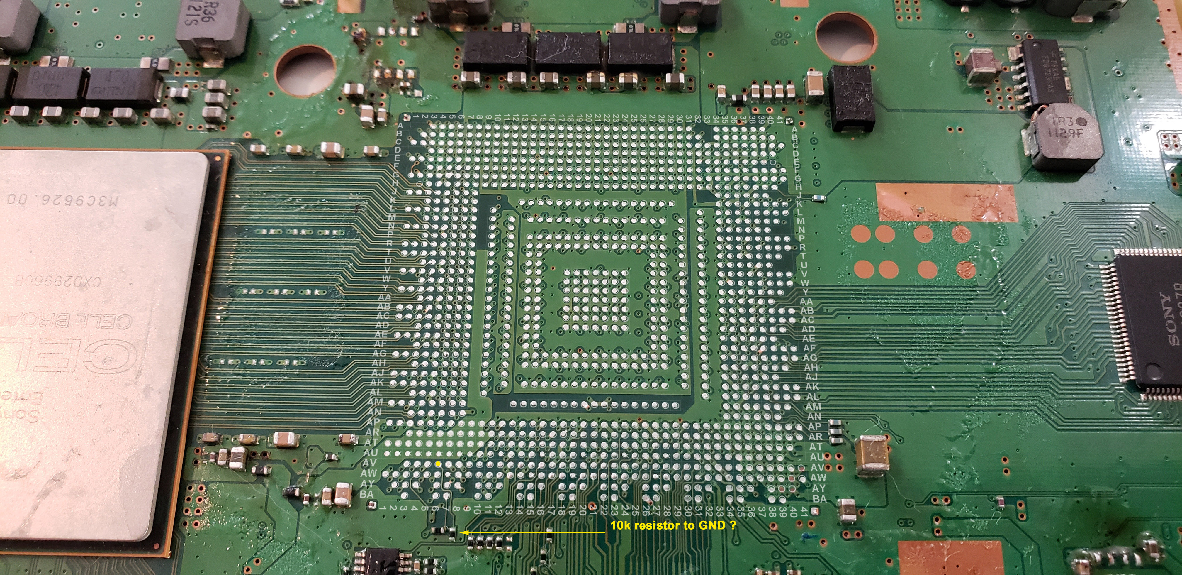
- Tying R2054 to GND with a 10k resistor (pull down resistor) prevents the RSX reset signal from triggering a CG reset on BGA pad AV6, without affecting reset on pad AW5. It looks like the arrow in the scematic is an incoming signal from the SYSCON. So this prevents the SYSCON from triggering CG_Reset. Why? IDK
- Evidently, the 65nm and 40nm RSX do not ever need CG reset. You can see SONY has it tied to GND with that 10k in the KTE-001 image. So the Frankenstein mod is simply copying that. I have no idea what function CG_Reset is supposed to serve in BC 90nm models. I wish I knew.
Ok, good to know sony already used the CG codenames in other lines of the service manuals with the meaning of clock generator, then im in the same boat, is our best guess
The fact is the names of the signals i was talking about belongs to syscon (not to RSX), as example there is another syscon line named SB_CGRST, in theory is should do exactly the same than RSX_CGRST but with the southbridge
And yeah, maybe this signals are used to initialize and sync them... im guessing the bittraining could start by using this reset signals, this way you are sure the syscon is "catching" them at the exact time interval to start the bittraining
The resistor to ground should be mostly to dont keep the line "floating" in an unestable state that could generate random resets caused by interferences, noises, etc...
I have not tryed to follow the line in the different motherboard models, but in the service manual of the SEM-001 it can be seen it have a resistor in between syscon and RSX named R2079... search for that in the .pdf is easy to find, it have some more resistors and capacitors related to it
There is also a resistor named R2054 located in between RSX_RESET and RSX_CGRST marked as xx (unpopulated, not present in retail units) that seems to indicate at some point they was joining together both signals... also, the circuit board allows to do that if we add that resistor, take a look at it because maybe the existence of that solder pads comes in handy for the frankies either to connect both together or to do the 10k resistor to GND to nerf the RSX_CGRST
As i said before, im not sure if this trick with the RSX_CGRST signal depends of the syscon model or the RSX model, but let me make a list of the motherboars that needs to be checked to find this:
DIA-002 (PS3 models CECHJxx or CECHKxx) <--- first PS3 model with a 65nm RSX (and a RSX RAM VDDR of 1.0v)
VER-001 (PS3 models CECHLxx, CECHMxx, CECHPxx, or CECHQxx) <--- first PS3 models with a sherwood syscon
SUR-001 (PS3 model CECH-21xx) <--- first PS3 model with a 40nm RSX
The change happened in one of them, my guess is it happened in VER-001 because they had to rewrite the syscon firmware for sherwoods, it looks like the perfect timing to modify the bittraining in between CELL, RSX and SB
")


 40nm RSX (CXD5300) about 1 month ago from a Chinese eBay seller, after 1 week they told me they had no "new" ones left in stock and only used / refurbished ones. So i said send it anyway, well it arrived today and check this out...
 ...and hey i got a few extra MLCCs for free!

