would be nice if you could take measures with a caliper
Here's what I found my A01 years later after sending it to Sony. A lightning strike fried it a week after I brought it home December 2006. I sent it in under warranty, got it back and enjoyed it for 6 years. Opened it years later to find this behind the CPU.


Sent from my iPhone using Tapatalk
You are using an out of date browser. It may not display this or other websites correctly.
You should upgrade or use an alternative browser.
You should upgrade or use an alternative browser.
sandungas
Developer
I wrote some posts talking about them here:Interesting... I had seen the plug before, but not those plates. Were they meant to be installed between the clamps and the board? It almost looks like the "official implementation" of the eraser mod.
https://www.psx-place.com/threads/t...out-removing-the-ihs.23066/page-6#post-260365
But this drawings resumes it pretty well
Because an image worths hundred words...
Without that piece, all the pressure is transfered to this points

And with the piece this way:

*Im assumming the white piece doesnt really touches CELL
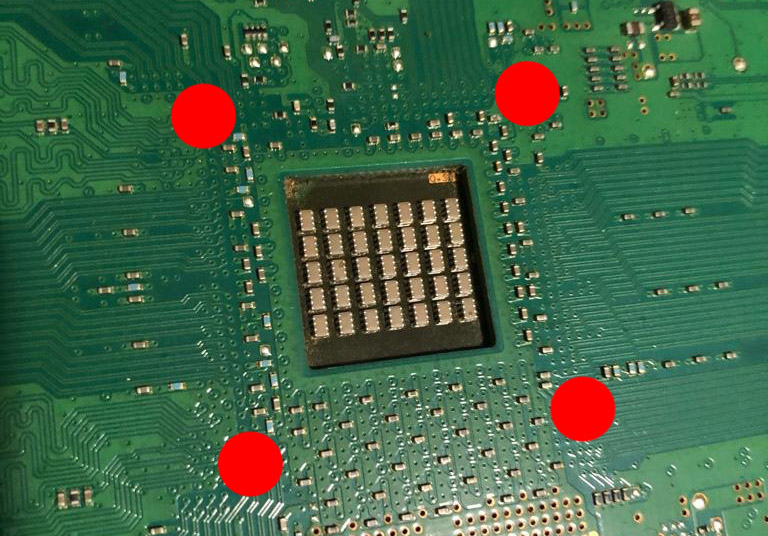
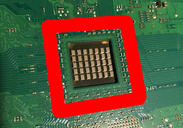
Basically... the 4 "bumps" at the corners are not optimal to transfer pressure
Is the same phisical rule that applyes if 1) place the hand on top of a table 2) place 1 kilo of rice on top of the hand 3) doesnt hurts (because the pressure generated by 1 kilo is spreaded in a big area)
But repeat the same experiment by placing a nail vertically in between the hand and the kilo of rice... this hurts because the pressuree is concentrated in a small point... well try again with a needle and it will enter in your flesh like butter
 (but is the same kilo = same pressure)
I mean... in theory the bumps are a bad solution... it would be a lot better to replace the bumps by some kind of "wall" all around the CELL peripheral (matching exactly with the most external border rows of BGA solders)
They was not able to do that because there are lot of tiny components around the "bumps"
And the other (huge) problem is the motherboard "hole" at the CELL center... is bad in many ways, not just because they cant "push" the CELL at the center but also because is reducing the structural resistance of that area a lot
This piece of plastic is intended to solve the second problem, and imo it should do it very well, but his thickness needs to be calculated very accuratelly (should be exactly the same height than the 4 bumps at the corners)
DeadEnd
Senior Member
would be nice if you could take measures with a caliper
But I have already posted the measurements before... At least of the plastic. Did not look at the corner balls though...


View attachment 38090
Edit: Corrected STL file, previous measurements were off.
Attachments
Last edited:
cfreddykrueger
Member
But I have already posted the measurements before... At least of the plastic. Did not look at the corner balls though...
View attachment 38089
View attachment 38088
View attachment 38090
Here is STL file for 3d printing (Untested)
I appreciate you taking measurements. At the time I had my system apart I never thought to do that. Is there a reputable 3-D printing service that would make this?
Sent from my iPhone using Tapatalk
haxxxen
Developer
just sharing my opinion about these 4 bumps on the backplates of CELL and RSX. if you are working on mainboard lying on back shield, be careful with these bumps, cause I have ripped off MLCC's, first on my 1400A and then also on my CECHL. afterwards I even have removed the plastic bumps, to never let it happen again
I appreciate you taking measurements. At the time I had my system apart I never thought to do that. Is there a reputable 3-D printing service that would make this?
Sent from my iPhone using Tapatalk
Problem with this are the materials that could withstand the temps, nylon would be the best option but is expensive (not everybody have nylon at home)
marciolsf
Member
I wrote some posts talking about them here:
https://www.psx-place.com/threads/t...out-removing-the-ihs.23066/page-6#post-260365
But this drawings resumes it pretty well
Basically... the 4 "bumps" at the corners are not optimal to transfer pressure
Is the same phisical rule that applyes if 1) place the hand on top of a table 2) place 1 kilo of rice on top of the hand 3) doesnt hurts (because the pressure generated by 1 kilo is spreaded in a big area)
But repeat the same experiment by placing a nail vertically in between the hand and the kilo of rice... this hurts because the pressuree is concentrated in a small point... well try again with a needle and it will enter in your flesh like butter
I mean... in theory the bumps are a bad solution... it would be a lot better to replace the bumps by some kind of "wall" all around the CELL peripheral (matching exactly with the most external border rows of BGA solders)
They was not able to do that because there are lot of tiny components around the "bumps"
And the other (huge) problem is the motherboard "hole" at the CELL center... is bad in many ways, not just because they cant "push" the CELL at the center but also because is reducing the structural resistance of that area a lot
This piece of plastic is intended to solve the second problem, and imo it should do it very well, but his thickness needs to be calculated very accuratelly (should be exactly the same height than the 4 bumps at the corners)
I sorta see your point… are you saying the mlcc's are the "needle"? I'd think the solution for that would be to increase the diameter of the balls (to spread the load, like you said), but like someone else pointed out, nylon can be hard to procure…
Victor Hugo Alvarez
Forum Noob
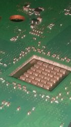
Here's what I found my A01 years later after sending it to Sony. A lightning strike fried it a week after I brought it home December 2006. I sent it in under warranty, got it back and enjoyed it for 6 years. Opened it years later to find this behind the CPU.
Sent from my iPhone using Tapatalk
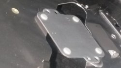
Bro you trying to prove what I say was wrong? First of all Does this plastic Cover Even has enough Thickness to Fully Fufill that Gape and give some kind of Pressure??? That must be Tested and measured in thickness, for me that plastic mostly Look like an isolation Protection Not only to the Protection of the Cell back extremely dangerous Short wise exposed Capacitors but aswell as the Exposed Entrance to the ~ 1.300 Bgas that 90nm Cell Cxd2964XXx has.
Victor Hugo Alvarez
Forum Noob
Guys if somebody Wonder about the Black Plastic Cell yes theyré indeed special, I dont think I can find where is the site I read that but I remenber that The Black Plastic Cell has that beyond obvious indeed has an very thin self pcb, that Cell indeed was said to Have Special more Electric conductable Material in its Pcb maybe that Little last Cell model only find in the Ss PS3s is an Continuation of that Black Cells maybe.
_XBrD4shDOE_808_
Member
Victor em nenhum momento ele disse que você esta errado, apenas está mostrando um detalhe que ele encontrou em seu aparelho que é raro de ser encontrado e foi posteriormente removido da linha de montagem. Provavelmente no inicio o PS3 vinha com essas tampas com o objetivo de presionar o CELL ou outro motivo qualquer, talvez proteger as mais de 1000 BGA's mas podem ter percebido que essa pressão causaria danos ao processador e que foi removido para que não ocorresse o que ocorreu com você.Bro you trying to prove what I say was wrong? First of all Does this plastic Cover Even has enough Thickness to Fully Fufill that Gape and give some kind of Pressure??? That must be Tested and measured in thickness, for me that plastic mostly Look like an isolation Protection Not only to the Protection of the Cell back extremely dangerous Short wise exposed Capacitors but aswell as the Exposed Entrance to the ~ 1.300 Bgas that 90nm Cell Cxd2964XXx has.
translation to english:
Victor never once said you are wrong, he is just pointing out a detail he found on his device that is rare to find and was later removed from the assembly line. Probably at the beginning the PS3 came with these covers in order to press the CELL or any other reason, maybe protect the more than 1000 BGA's but they may have realized that this pressure would cause damage to the processor and that it was removed so that what happened would not happen. with you.
sandungas
Developer
No, im my example the needles are the 4 plastic "bumps" of the cornersI sorta see your point… are you saying the mlcc's are the "needle"? I'd think the solution for that would be to increase the diameter of the balls (to spread the load, like you said), but like someone else pointed out, nylon can be hard to procure…
Using another example... is like a bridge with 2 columns, if we add lot of weight on top of a column is fine, but if we add lot of weight in between the 2 columns the bridge could break (because the pressure is deforming it)
In a idealistic world we would like to spread the pressure in the biggest area posible (never exceding the IHS at the other side of the board), but it needs to be made with a solid material so all that mlcc's around are a problem, when they designed the motherboard they only keept this areas clean of components
Note the circles i painted are way bigger than the plastic bumps... they made the plastic bumps smaller just because they didnt want to get too close to any component
But it would be a lot better to do it this way, you know this is one of the cases where a rough design wins
Im just talking theoretically because the square i painted in this last drawing is on top of some components, so is not posible to do it with a solid material (at the risk of cracking some mlcc's)
We could make the bumps a bit bigger using a solid material like nylon (or any other plastic, it doesnt matters much)
Or like in the second drawing, but i painted on top of some components so the material should be flexible to dont damage the mlcc's (a big square of rubber)
sandungas
Developer
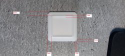
I have a photo over here handy to see how it looks at the other side
The 4 factory plastic bumps are concentrating 100% of the pressure on this small dots
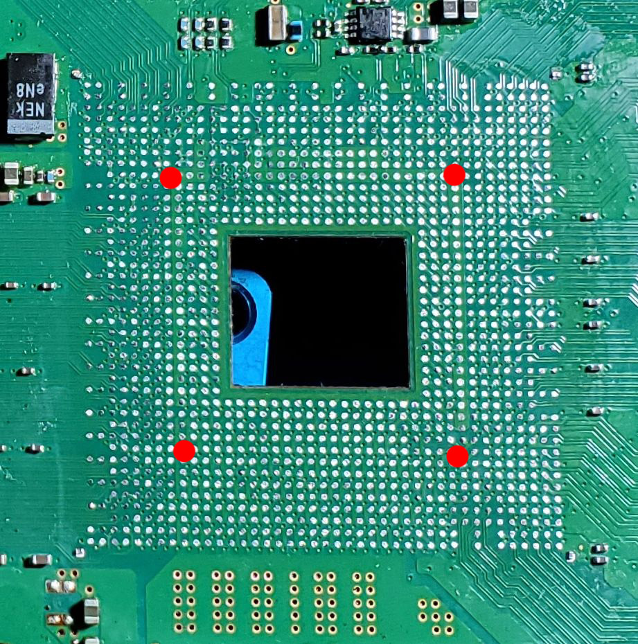
But idealistically... is a lot better to spread the pressure all around the BGA solders evenly
The withe squared plastic piece made by sony prevents a bit the deformations at the inner borders of the "hole" but doesnt solves the problem completly
The 4 factory plastic bumps are concentrating 100% of the pressure on this small dots
But idealistically... is a lot better to spread the pressure all around the BGA solders evenly
The withe squared plastic piece made by sony prevents a bit the deformations at the inner borders of the "hole" but doesnt solves the problem completly
I don't think that you would need the full square to give it the needed rigidity
With something like this should be enough:

(if the support sustrate is completely flat)
That gives the idea that with a bakelite plate laser cutted you could skip any component and create a custom support without the need of covering the middle hole
With something like this should be enough:
(if the support sustrate is completely flat)
That gives the idea that with a bakelite plate laser cutted you could skip any component and create a custom support without the need of covering the middle hole
Last edited:
Victor Hugo Alvarez
Forum Noob
Alright Sorry I should Not have used that words and still think that 2 mm Thickness from Cell Pcb to the back metal Plate will have 0 Pressure cause 2 mm May Be Only be touching that back plate, I Will open one of my PS3 to Measure it.Victor em nenhum momento ele disse que você esta errado, apenas está mostrando um detalhe que ele encontrou em seu aparelho que é raro de ser encontrado e foi posteriormente removido da linha de montagem. Provavelmente no inicio o PS3 vinha com essas tampas com o objetivo de presionar o CELL ou outro motivo qualquer, talvez proteger as mais de 1000 BGA's mas podem ter percebido que essa pressão causaria danos ao processador e que foi removido para que não ocorresse o que ocorreu com você.
translation to english:
Victor never once said you are wrong, he is just pointing out a detail he found on his device that is rare to find and was later removed from the assembly line. Probably at the beginning the PS3 came with these covers in order to press the CELL or any other reason, maybe protect the more than 1000 BGA's but they may have realized that this pressure would cause damage to the processor and that it was removed so that what happened would not happen. with you.
Victor Hugo Alvarez
Forum Noob
Yes Absolutely it consumes less Power and It heats far less cause the Fat PS3S heatsinks are far bigger than the Slims PS3s and as you shall know as the 40nm GPUs of slims consumes less Energy to work due to the newer smaller 40 nanometers transístors size it generates less heat than the old GPUs with bigger transístors, just basic eletronics.so does this mean the ps3 would consume less power? what would be the benefits? whats the last gpu supported? slim?
Victor Hugo Alvarez
Forum Noob
Victor em nenhum momento ele disse que você esta errado, apenas está mostrando um detalhe que ele encontrou em seu aparelho que é raro de ser encontrado e foi posteriormente removido da linha de montagem. Provavelmente no inicio o PS3 vinha com essas tampas com o objetivo de presionar o CELL ou outro motivo qualquer, talvez proteger as mais de 1000 BGA's mas podem ter percebido que essa pressão causaria danos ao processador e que foi removido para que não ocorresse o que ocorreu com você.
translation to english:
Victor never once said you are wrong, he is just pointing out a detail he found on his device that is rare to find and was later removed from the assembly line. Probably at the beginning the PS3 came with these covers in order to press the CELL or any other reason, maybe protect the more than 1000 BGA's but they may have realized that this pressure would cause damage to the processor and that it was removed so that what happened would not happen. with you.
Hey Im pretty Sure that plastic Sony used dont give any Pressure at all, as it have just 2 mm thickness and as I see the gape between Cell Pcb and back metal plate is about 3 mm tall, if that plastic sits Up in the Cell back Capacitors then that will give Pressure But I cant remenber the exactly draw of that plastic but if I remenber right the Plastic has an design that is made to not Even touch the Capacitors in Cell Back.
Yea looking at the photos @DeadEnd posted that plastic model will not give any Pressure at all on Cell cause It sits on Cell Pcb and as 2 mm Thickness and the gape between Cell Pcb and the back metal plate is much bigger than 2mm, im pretty Sure must be 3 or nearly 3 mm, I dont have any rule right now but I know about milemeters cause I draw everyday some arts using rulers so trust me the gape is much more than 2mm and must be 3 mm so zero pressure.
Attachments
Last edited:
Victor Hugo Alvarez
Forum Noob
Hey Im pretty Sure that plastic Sony used dont give any Pressure at all, as it have just 2 mm thickness and as I see the gape between Cell Pcb and back metal plate is about 3 mm tall, if that plastic sits Up in the Cell back Capacitors then that will give Pressure But I cant remenber the exactly draw of that plastic but if I remenber right the Plastic has an design that is made to not Even touch the Capacitors in Cell Back.
Yea looking at the photos @DeadEnd posted that plastic model will not give any Pressure at all on Cell cause It sits on Cell Pcb and as 2 mm Thickness and the gape between Cell Pcb and the back metal plate is much bigger than 2mm, im pretty Sure must be 3 or nearly 3 mm, I dont have any rule right now but I know about milemeters cause I draw everyday some arts using rulers so trust me the gape is much more than 2mm and must be 3 mm so zero pressure.
Motherboard is about ~1,5 mm thickness and Cell Bga is maybe 0,5 mm ~ 0,4 mm soldered so 1,9 mm gape already and then you have the gape between Motherboard Pcb and Back Plate due to the 4 spacers in the back plate, the spacers must have 1 mm thickness, so the gape between Cell Pcb and back plate is Really 2,9mm to 3 mm, so if the Rare plastic really is 2mm thick as measured by Deadend then theres absolutely Zero x Zero pressure on Cell Die and actually that plastic Gape my Even be Loose when you move the PS3 lol.
sandungas
Developer
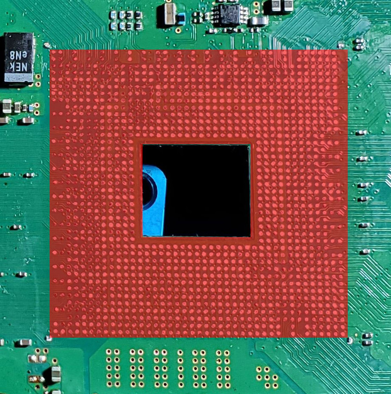
The gap in between the motherboard surface and the squared metal piece should be exactly the same height of the 4 plastic bumps that can be seen at the corners of this photoYea looking at the photos @DeadEnd posted that plastic model will not give any Pressure at all on Cell cause It sits on Cell Pcb and as 2 mm Thickness and the gape between Cell Pcb and the back metal plate is much bigger than 2mm, im pretty Sure must be 3 or nearly 3 mm, I dont have any rule right now but I know about milemeters cause I draw everyday some arts using rulers so trust me the gape is much more than 2mm and must be 3 mm so zero pressure.
And it should match with the thickness meassured at left in this photo by @DeadEnd
In other words, the gap in between the motherboard surface and the squared metal piece is 1mm
Think in it this way... if the height of the plastic bumps was bigger then the plastic piece would be "floating" and moving around, thats bad
And if the thickness of the pàlstic piece is bigger than the bump heights then the bumps woould not make any function because would not touch the motherboard
sandungas
Developer
Look, we can use this photo as reference, at some point someone needs to meassure the height of the 4 plastic bumps accuratelly... but in the meantime this comparison gives a rought approach
Im measuring the shadow of both, the 4 plastic bumps, and the thickness of the squared plastic piece... overall seems to be the same, and @DeadEnd said thats 1 milimeter
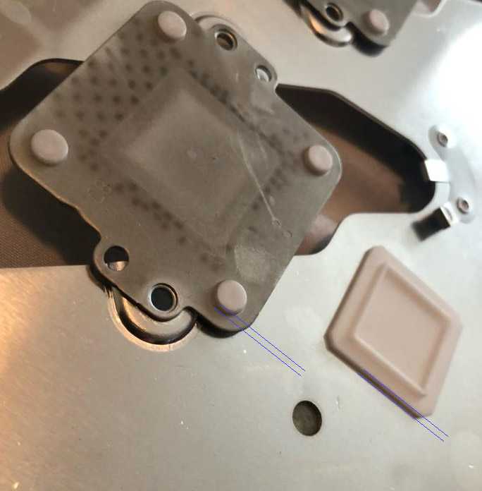
*btw, keep in mind the height of the 4 plastic bumps could be different for every motherboard... when they was using the squared plastic piece the height of the 4 bumps should match with it... but when they stopped using the squared plastic piece they had more freedom to change the height of the 4 bumps
Im measuring the shadow of both, the 4 plastic bumps, and the thickness of the squared plastic piece... overall seems to be the same, and @DeadEnd said thats 1 milimeter
*btw, keep in mind the height of the 4 plastic bumps could be different for every motherboard... when they was using the squared plastic piece the height of the 4 bumps should match with it... but when they stopped using the squared plastic piece they had more freedom to change the height of the 4 bumps
Similar threads
-
-
 PS3 PS3 CECHA RSX Swap (40nm) – JP Limited – SYSCON Patch, VDDC Mod – Need Detailed Help
- Started by jw0710
- Replies: 4
-

-
