Awesome, thats lot of 3D design work, im used to design and build things (sometimes with my own hands) and i know very well the sane state of mind is to consider every attempt as a "prototype". Because even if you dedicate lot of time in the design stages and your first built prototype is fully functional eventually you will feel the need to do "prototype v2"... and so on

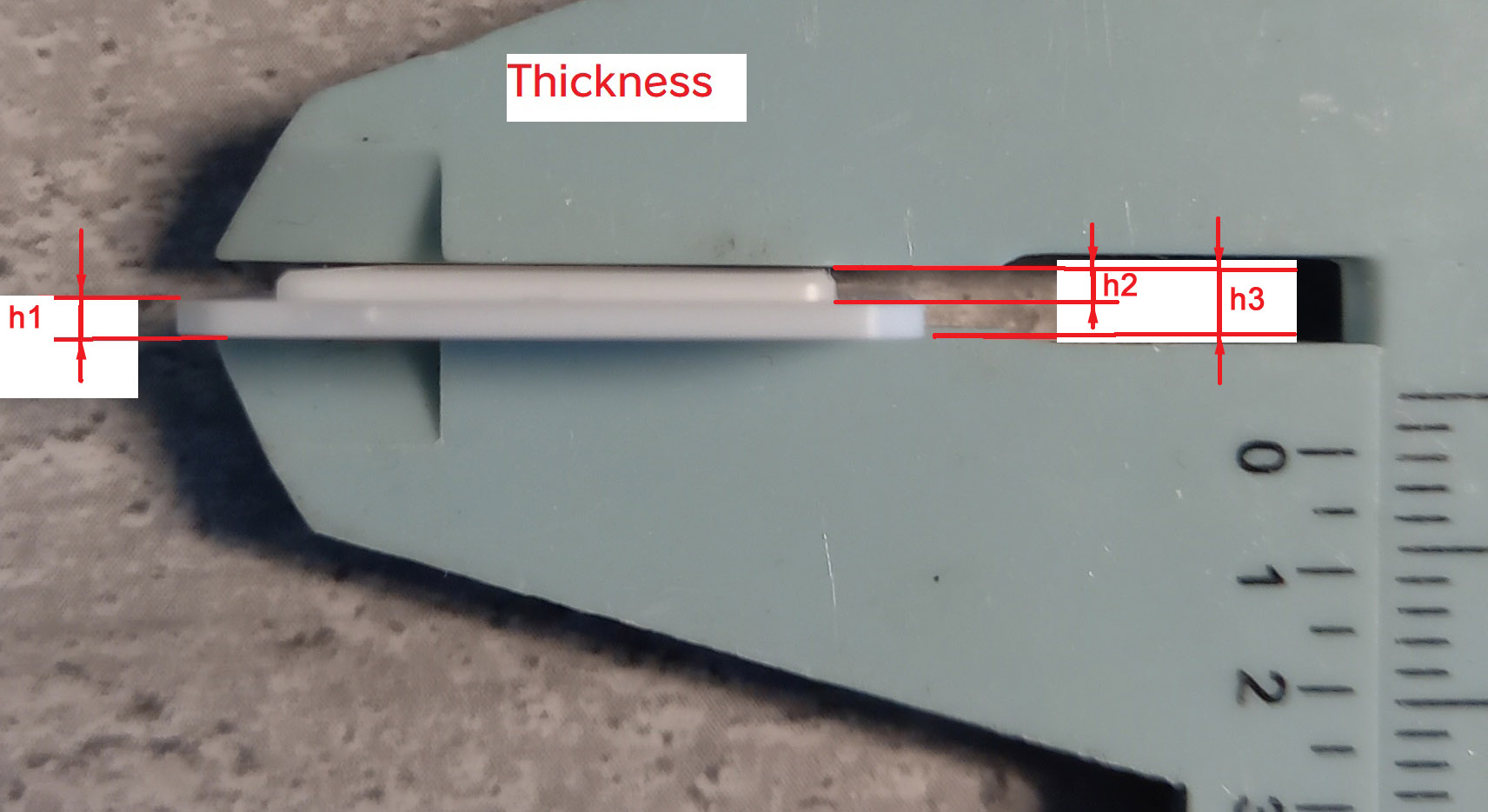
My approach (without a 3D printer) would be to build the plastic piece without the MLCC details, and then use a drill to create the "holes" for the MLCCs manually, you know, the MLCC are little rectangles and a drill is going to create a circle, but thats fine because the amount of removed material (the differences in between a rectangle and a circle) would be small. In your photo with that long "channels" you are removing more material
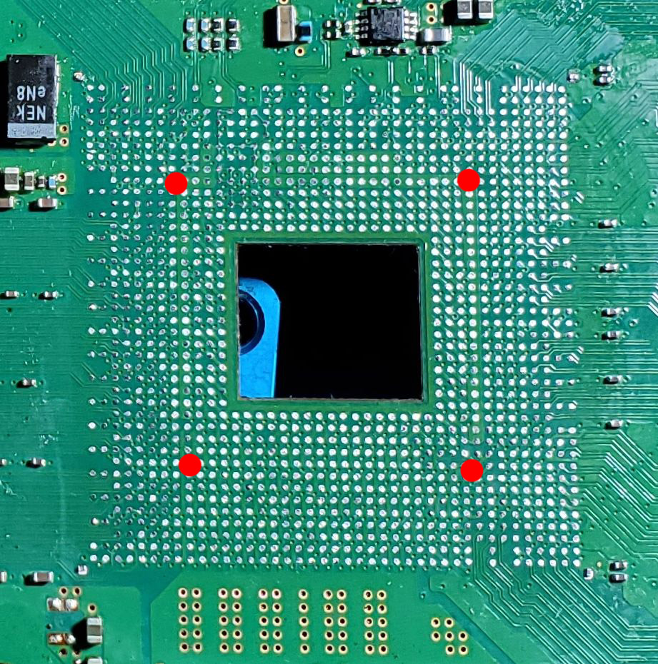
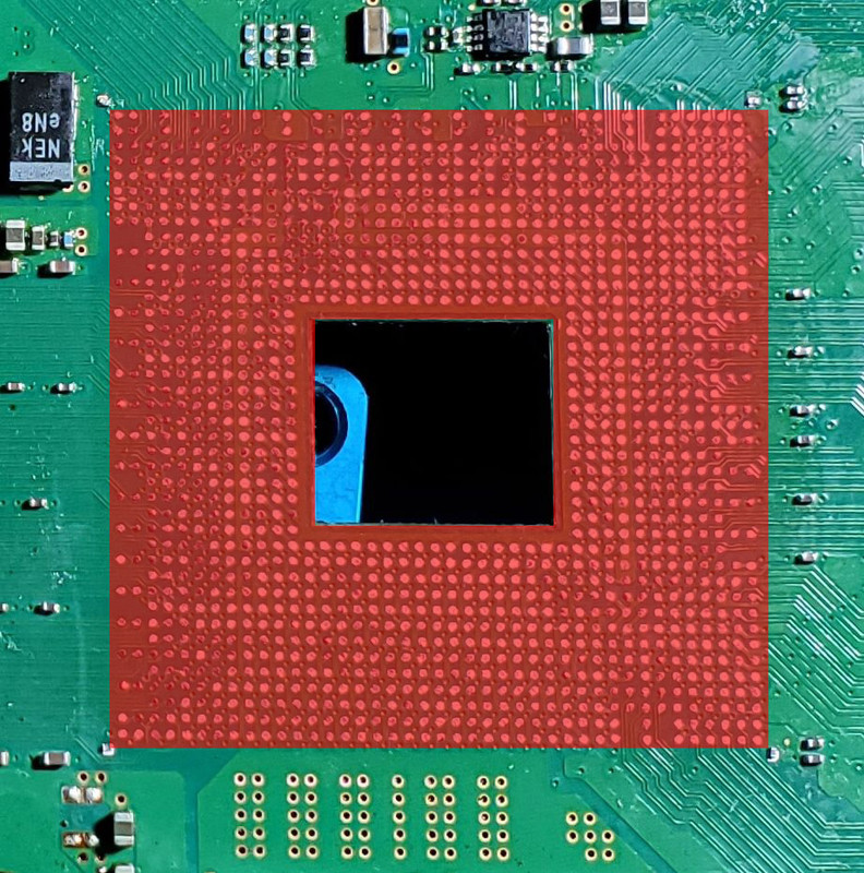
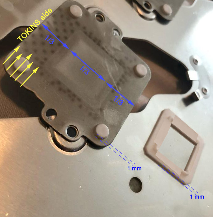
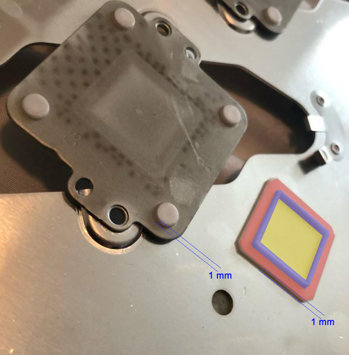
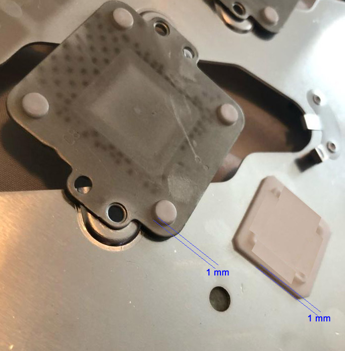
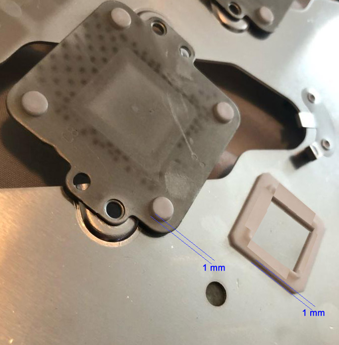
All this time i been doing rought calculations because i dont have the parts, and im repurposing some of the photos posted here by others (some of them are from a DIA-001), so im not completly sure about the meassures but today i tryed to "transfer" the dimmensions of the metal square to your plastic piece and doesnt looks bad, is a bit like this, right ? (the metal is represented by the yellow square)
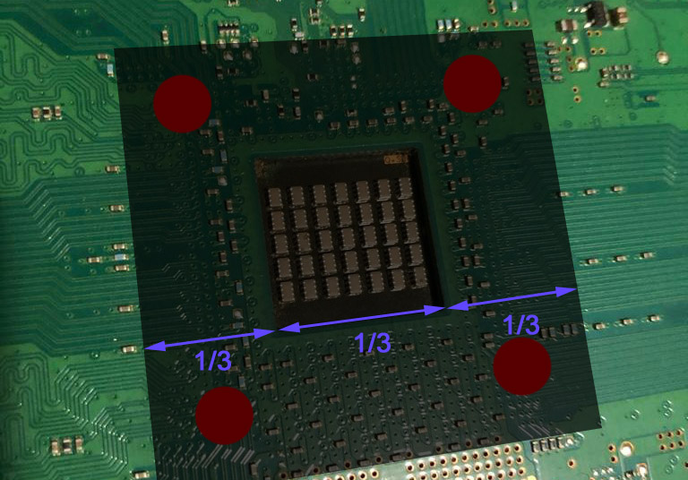
For curiosity sake... im repurposing this photo (again) using the rule of 1/3... and marked the "rows" of MLCs of the tokin side for comparison purposes. Note how i aligned the yellow square of the previous photo with the "fifth row" of MLCCs of the tokin side
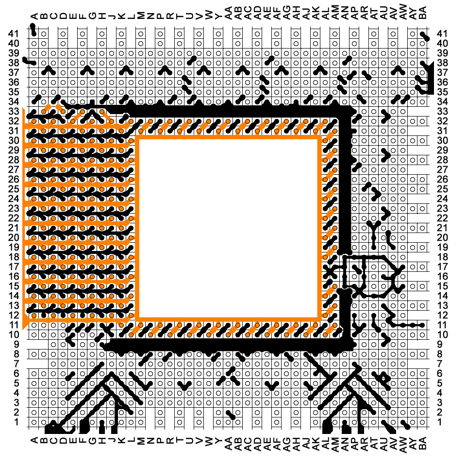
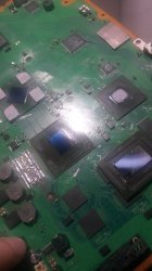
Btw, that brown marks in the photo indicates there is a lot of heat in them and are really close to the metal, i think it could be a good idea to use thermal silicone all along
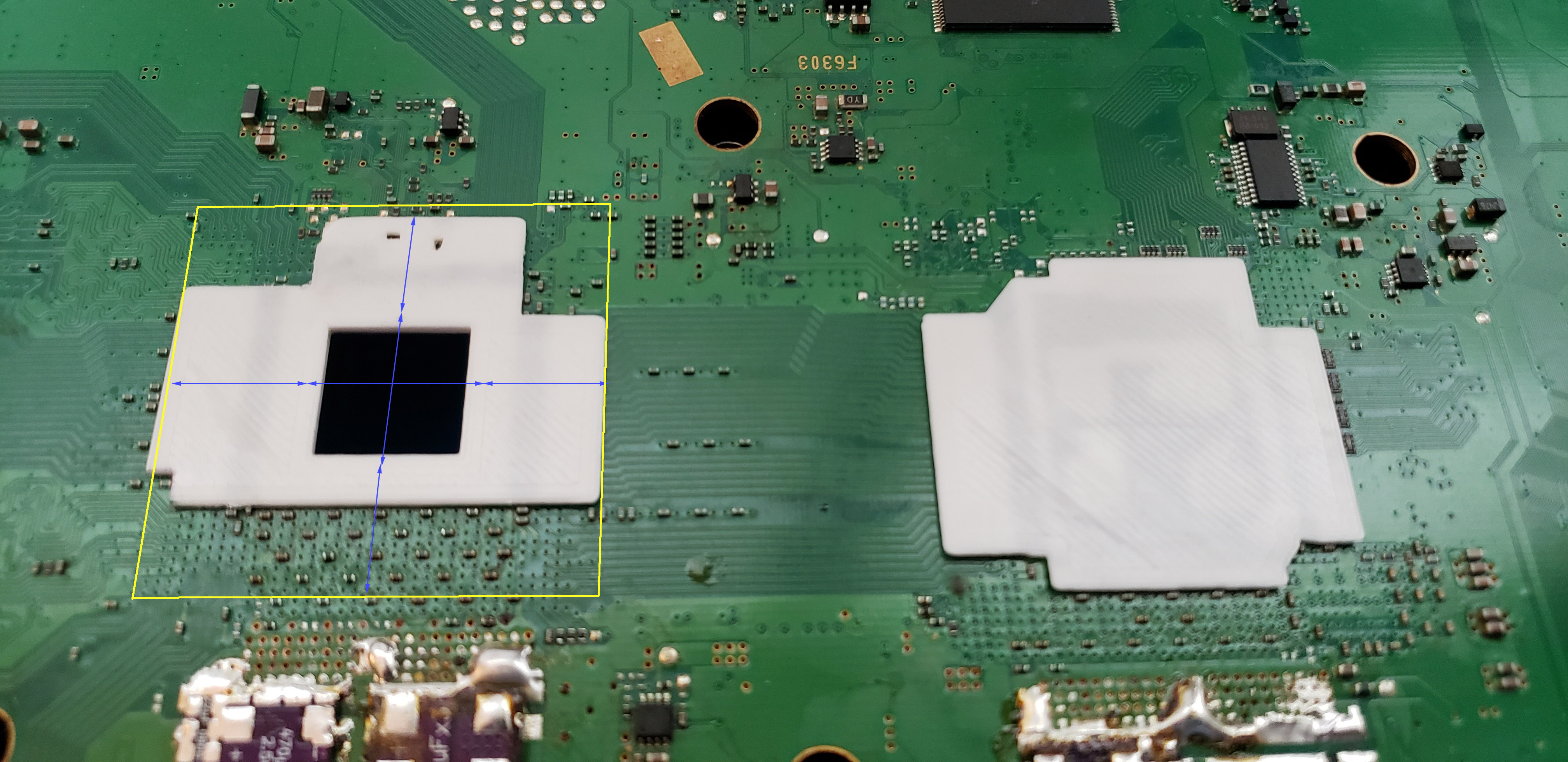
Btw, this plastic piece can be used in all PS3 models, but the design depends at least of 4 groups because the size of the motherboard "hole" depends of the CELL generation (90nm, 65nm, 45nmv1, 45nmv2)... and additionally the location of the MLCCs could vary by motherboard model
But this involves adding plastic in between the bottom surface of the heatsink and the motherboard surface, right ?... if thats the idea i have to tell honestly that i dont like it because is going to reduce the pressure, unless is calculated with huge preccision of decimals of milimeters
If your plastic piece is 0.1mm smaller then is pointless (because there is no pressure transfered to your piece), but if is 0.1mm bigger then is going to take some of the pressure that originally was applyed to the BGA (so you are reducing the pressure on the BGA)
-----------------
Bonus
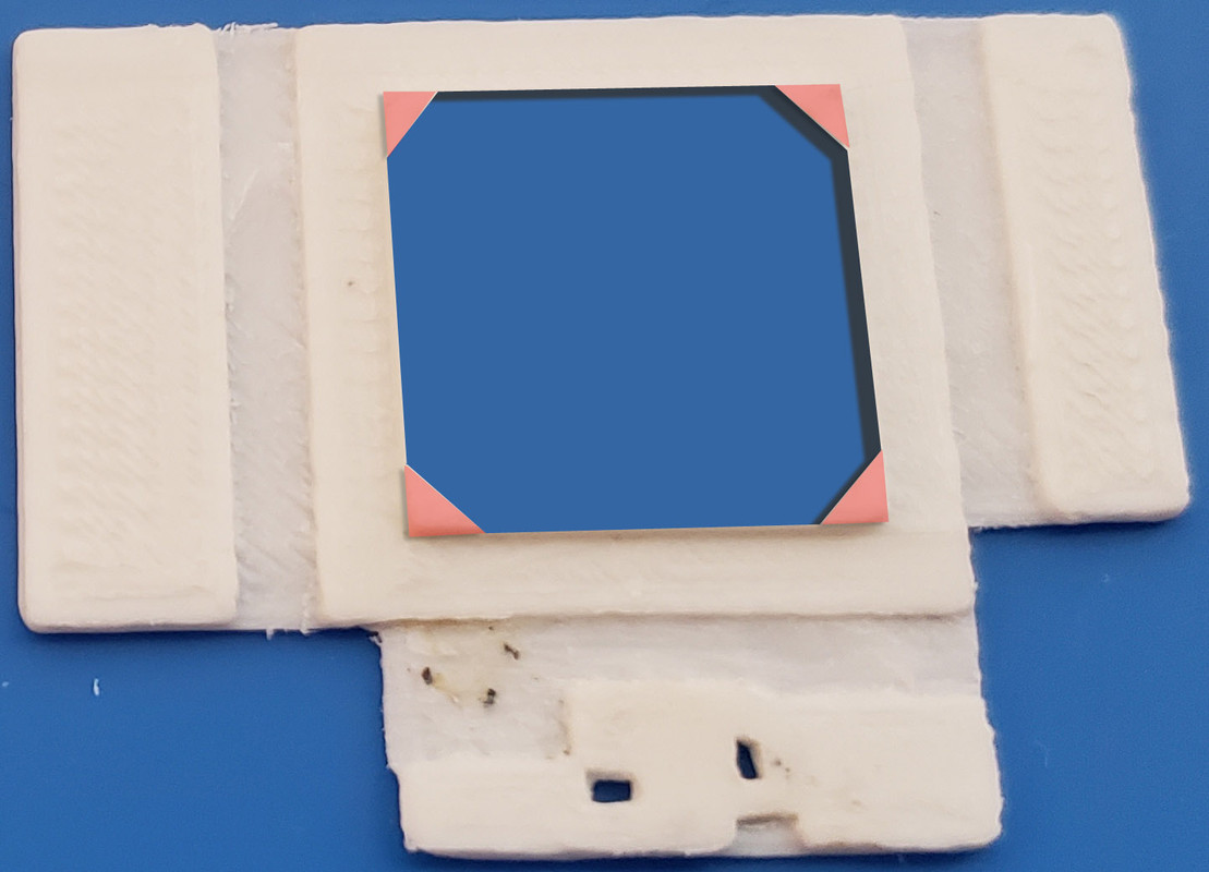
Im using your photo to show the reduction of material i mentioned before, you know... im removing a lot of the "vertical walls" (only intended to align the plastic piece with the motherboard), and instead of them im only keeping 4 little triangles at the hole corners, i think thats enought (and is also the minimal way to do it)
Is not only a matter of reducing the amount of material, but also to "open" the hole as most as posible because it seems there is a lot of heat in that area, and is better to remove the plastic to allow the heat to be transfered to the metal square (and indirectly to the whole metal shield)
In the official plastic piece made by sony there is not a hole, but we agree in doing it because is a hot spot

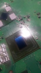
Actually i noticed in your photo you are experimenting with a thermal pad inside the hole, yeah, i like it
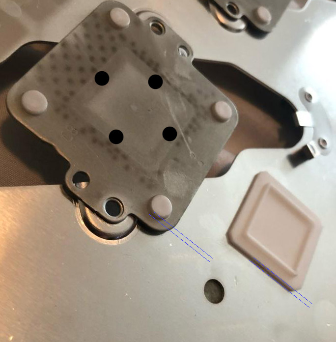
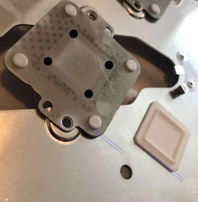
Another way to improve that would be to drill 4 holes in the metal squared piece (the holes needs to be simmetrical, so there are only 2 ways to do it)
@ElGris was asking my oppinion about this idea some weeks ago, but he was suggesting to use a fan or some air duct to force the air to pass under CELL
Well... the point is... the holes in the metal im suggesting are not inteded to create an airflow below CELL BGA balls because the air always contains particles of dust, and that particles are going to end sticked to the BGA balls, and this could be a big mistake
My idea of the holes in the metal squared piece is mostly because this way the hottest air can "escape" from that prison easilly... you know... it should happen naturally but cant be considered an airflow
-----------------
Merged posts
Just to be clear... i mean this:
Or this:
The black circles represents holes that needs to be drilled into the squared metal piece. Basically, are going to weaken the rigidity of the metal, but allows the hottest air to move away


")