PS3 Frankenstein PHAT PS3: CECHA with 40nm RSX

Im partially responsible of what i publish in wiki and i dont feel confident in publishing that, sorry, it looks more like a pareidolia
o-JESUS-DOG-BUTT-570.jpg


What makes me think this is very unprobable is what i mentioned before
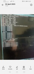
By reading what you are saying it seems in RSX they went so far away up to "GB" -> "AGB" -> "BGB" -> "CGB" -> DGB -> EGB -> FGB -> GGB

It would mean there is (at least) 8 revisions of the CXD5300xxxx series. Even considering some of the intermediate models im mentioning could be prototypes of rarities that was not produced massivelly, 8 is too much
 
I am sorry the picture quality is so bad. I did not know you guys would be interested and shipped the console out before I was asked for that.

I am for sure know it is CXD5300GGB. @Computer Booter had one too. I am not a foolish man my brother I can read! It was very clearly visible on the IHS, it was only not well captured by the camera, and if I still had the unit, I would take a better picture for you.

Kind Regard,
Josh
 
Im partially responsible of what i publish in wiki and i dont feel confident in publishing that, sorry, it looks more like a pareidolia
o-JESUS-DOG-BUTT-570.jpg


What makes me think this is very unprobable is what i mentioned before


It would mean there is (at least) 8 revisions of the CXD5300xxxx series. Even considering some of the intermediate models im mentioning could be prototypes of rarities that was not produced massivelly, 8 is too much
8CBEAE31-AF7B-436A-B01E-F26C24F7C145_compress56.jpg

74EF3A44-C75A-4515-A2E1-A0E76387DC1C_compress33.jpg
Also this is one of those boards that have that black plastic protection for the CPU
 
Dont take wat i said as something offensive, but you know what happens, this processes used to etch or print names in electronic components are not much precise, and eventually it could happen that some particle or chemical "lands" in the surface and converts an 8 into a B... or a G into a 6.. or whatever
Sometimes the only way to be 100% sure about the name is to look at other component where the name is more "readable"
But in that photo is clear @Pacorretaco

I uploaded the report in this list (note the serial number of the motherboard is lower than others JSD-001, interesting):
https://www.psdevwiki.com/ps3/RSX#Types_.40_SKU.27s
Uploaded the image here:
https://www.psdevwiki.com/ps3/File:RSX_CXD5300GGB.png
Created a new page specific for it (the list that appears at top with other RSX models is a bad idea we keep doing)
https://www.psdevwiki.com/ps3/CXD5300GGB
And added a link to the new page in the templates that appears in main page
https://www.psdevwiki.com/ps3/Template:Motherboard_Components
 
Would a APS-231 in a CECHAXX (with a 40nm RSX) be ideal due to the reduced power requirements or is a APS-226 still recommended?
 
Hi I have a cok002 which I've reballed with a 40nm rsx I've done the hardware mods voltage /resistor.

But I think I've screwed the syscon training up ..

I can't seem to fix the checksum no matter what I do, if anyone could possibly help I'm stuck,

Addr: 0x000032fe should be 0x647c
Sum: 0x1800
Addr: 0x000034fe should be 0x5915
Addr: 0x000039fe should be 0x0038
Addr: 0x00003dfe should be 0x00ff
Addr: 0x00003ffe should be 0x00ff

I will try to upload a photo of log, apologies if this is wrong place to post
Screenshot_20230425_110522_com.android.chrome.jpg
 
Would a APS-231 in a CECHAXX (with a 40nm RSX) be ideal due to the reduced power requirements or is a APS-226 still recommended?
Both will work fine.
Just that the APS 231 will have less headroom, as it is a cut down version of the 226.
The thing doesnt even have screws haha.

The lines directly after the "sum:0x..." lines are the ones that need to be modified.
So in your case from your last picture you should write:

w 34fe 15 59

Good luck
 
Thankyou for the help, I've had a look today and Im getting error 0xa0202102
Is this hdmi error, I'm not sure if it's due to the wrong 40nm training code or just failed reball, I will upload the log
Screenshot_20230426_094342_com.android.gallery3d.jpg
 
I'm lost I need some help
Thankyou for the help, I've had a look today and Im getting error 0xa0202102
Is this hdmi error, I'm not sure if it's due to the wrong 40nm training code or just failed reball, I will upload the log View attachment 40525
It is not related to the training data.
It is a failed reball sorry.

It is a difficult thing. Even some professionals cannot do it reliably. So you need a lot of previous practice reballing to be able to do it right, and without destroying.

From those errors it could be several things, but probably merged balls near the SYSCON corner, exploded VRAM possible also. You can check VRAM power rail resistance if you want, but the chip needs ro be lifted in any case
Ok thanks,

I have done 2 standard 90nm swaps successfully but they were fully working boards,

My bga set up is good, clean lifts every time, no pulled pads

reballing the chip I have perfected can do in one attempt no balls joining etc using reflow oven

So not a problem to try again until I get it right
I have a few 60nm chips I've pulled so I will retry with 60nm as I don't need the voltage mod and it's more streight forward

Is this diagram OK for good rsx testing?
Screenshot_20230401_155517_com.android.chrome.jpg
 
Yes you are looking at right diagram or can look after RIP-Felix signature link with different diagrams. As Pacco said earlier something is merged or popped ram that is not visible.

Sent from my M2007J20CG using Tapatalk
 
Yes you are looking at right diagram or can look after RIP-Felix signature link with different diagrams. As Pacco said earlier something is merged or popped ram that is not visible.

Sent from my M2007J20CG using Tapatalk
Thanks appreciate your help. I'm really happy though because I have made today a cok002 with 60nm chip , could you link the rip felix rsx chip test
 
Yes you are looking at right diagram or can look after RIP-Felix signature link with different diagrams. As Pacco said earlier something is merged or popped ram that is not visible.

Sent from my M2007J20CG using Tapatalk
So I've done a 60nm on cok 002, I can't get past this checksum
 

Attachments

  • Screenshot_20230427_160045_com.android.gallery3d.jpg
    Screenshot_20230427_160045_com.android.gallery3d.jpg
    313.4 KB · Views: 62
Well good funny thing how Sony put that situation
" should be "
I never asked why not " must be " [emoji848]
Probably people will put more accent there.
 
It is not related to the training data.
It is a failed reball sorry.

It is a difficult thing. Even some professionals cannot do it reliably. So you need a lot of previous practice reballing to be able to do it right, and without destroying.

From those errors it could be several things, but probably merged balls near the SYSCON corner, exploded VRAM possible also. You can check VRAM power rail resistance if you want, but the chip needs ro be lifted in any case
Hi paco I have made 60nm cok 002 :),

I have also try another 40nm on a cok 002 the reball i think is very good, but when I try syscon training I'm getting an MMIO access error? Is this bad other component?
Screenshot_20230429_083253_com.android.gallery3d.jpg
 
Back
Top