Yes, that's the post from Workz.
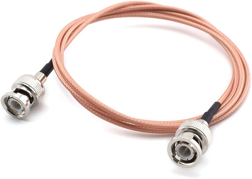
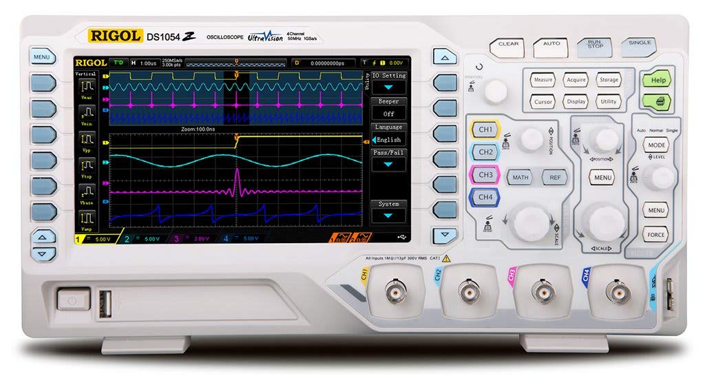
I just use a plain old probe, but I pop the grabber off the end to expose the needle probe underneath. I clip ground to the copper ground plane all around the edge of the board, and I just jam the probe in to the vias closest to the chipset after the TOKIN and hold it there. We're not looking for any kind of perfect measurements here, you're checking that the signal didn't clearly and fundamentally change over to either that weird sawtooth or a clear sine wave.
If I remember correctly from when I was dicking around with showing how many TOKIN you could remove entirely before it failed, I believe I got almost 500mv peak to peak of noise with half of them removed and still had a backwards compatible model running GT6 just fine. The vast majority of the noise was much smaller than that, but the instantaneous spikes were quite large.


")