PS3 (Research/Experimental) - NEC/TOKIN Capacitors Replacement - YLOD

PS3#7 Continued...
(RSX Reflow)​

This morning I reflowed the RSX. This attempt went really well, my best yet! I think I finally figured out how to keep the drafts from getting under tho MB while it's heating. I didn't want to allow air from my vent fan to be able to be pulled under the mother board. So I covered the whole board and IR preheater plate with Aluminum foil. Just the top of it, the vents to cool the preheater I left open, so the preheater's electronics can stay cool, but the air could only be pulled over the motherboard, which was covered in aluminum foil. Only the RSX was exposed. That's so I could use the hot air station with a 45x45mm BGA nozzel to heat it. However, while the board was baking and preheating, I used another piece of foil to comp,etely cover the top. That kept the temps on the top and bottom side within 20C of each other throughout the whole process. The idea is to minimize the temp difference, so it doesn't warp.

I spent the first hour at about 95C driving off the water. I know that @squeept likes to bake his boards for 24 hours, but IMO that's not entirely necessary. Moisture in the board boiling off actually takes heat with it and keeps the board cooler than the boiling point. Once the moisture is gone the temps begin to rise. That's when I know the board is dry. I live in a place with high humidity too, although today it's more like 40%. I noticed that after about 45 minutes at 95-100C the temps started to rise. I gave it a full hour just to be safe.

After the bake, I raised the preheater temp to to a setting that brought the bottom side probe to 150C. Once the temps stabilized I added amtech flux around the edges of the RSX, until it was thoroughly wet. Then I turned on the Hot air to begin raising the topside temps. This is where patients and practice come in. I raised both the hot air and preheater together until the board and topside read about 180C. Then I began raising the hot air only. At about 200C the RSX flowed and I confirmed this by nudging it gently with my forceps. Once I confirmed it was flowed I dropped the hot air to 200 which cooled the RSX pretty quickly. I estimate the RSX was above 190 for about 30 seconds to a minute tops. Then I moved the Hot air away and covered the top with aluminum foil again. The board was about 180C at this point.

I began the cooling cycle now by setting the preheater down to 150C and let it cool from 180C to 150C over 5-10 minutes. Then from 150C to 120C over the next 10 to 20 minutes. Basically, I'd set it down about 20-30C from it's previous setting and let it cool as long as it took to reach the set point, then set it down another 20-30C. Once it got below 100C I placed a hand towel over the foil to insulate the topside more and set it down to 50C. I waited until it reached 50 and turned the preheater off. Each time it took about 10-20 minutes to cool and all totaled it took maybe 1hr to1.5hrs to cool to room temp.

To clean the flux residue I used a combination of Acetone, electronic contact cleaner, and 99% IPA. I cleaned off the easy to reach Flux residue with IPA and cotton tipped applicators first. The stubborn burned on flux with acetone (goo gone). To get the flux underneath the BGA I used electronics contact cleaner, some really harsh chemicals in a spray can. But it has a tube and I can place the MB at an angle and run the fluid down the slope behind the RSX to get the flux out. I just placed a Paper towel underneath the bottom edge of the RSX as I did to soak up the solvent and dissolved flux that ran out from underneath. I flipped the board 90 degrees and repeated many times. Then I did the same with acetone. and again with IPA in a spray bottle. Lastly I went back over the whole board with IPA and a tooth brush to get every nook and cranny clean. I placed a paper towel over the board and ran the toothbrush over the top of the towel to soak up the IPA (if you let it dry on the board there will be a white residue from the dissolved flux). I repeated until I was satisfied it was thoroughly clean! Then I used compressed air to blow all the hiddin moisture out from underneath all the chips and caps (there's alot). It dried up pretty quick, but I caught alot of it with a paper towel. I touched up any white residue spots I missed with a cotton tipped applicator and IPA.

I have to say, the cleanup process is the most tedious part. I envy @squeept's ultrasonic IPA bath and drying oven...lol!

I confirmed with a multimeter that my solder was still intact on the Tantalum arrays and they were fine. I did cover these well with aluminum tape and foils to hopefully shield theyr solder from flowing. It seemed to work. Both CPU and RSX had about 3 to 3.5 ohms of resistance +/GND rail. That's healthy.

Results:
The console fired up immediately no problem and has been stress testing while I type this up. About an hour so far. No errors to report. I have not heard the fan ramp up beyond the second step and there are no graphical artifacts. I will continue testing, complete with cool down cycles to allow the board to relax and report back.

Just to remind you. The CPU has an array of 18x 270uF TaPol and the RSX has 12x 470uF TaPol using the SoulKilla PCB. The console is running fine with all Tantalum now. I have not looked at the oscilloscope, but it should be the same as it was in the last test. Nothing has changed, except the BGA defect is gone.

What's next?
First I need to install a larger HDD. Then I need to jail break, so I can set a custom fan curve. I'm working up a custom fan duct to adapt a Noctua 40mm fan over the power supply. It will duct cool air from the front panel multimedia port, which is useless anyway. I already spliced the fan connector into the BR 12V pwr connector. So it automatically starts spinning when the console is powered up. I just need to finalize the 3D model for the duct. It's very alpha ATM.

The reason for the PSU fan/duct is because I intend to cut a hole in the bottom of the shell to allow cool air to be directly pulled in by the heatsink fan. That works great to cool the CPU/GPU, but it causes the PSU to over heat. So the fan is to prevent that.

I gotta say, I have been messing around with the hardware and trying to fix consoles for so long, I never get a chance to actually play games! So now that I FINALLY have a successful Tantalum system, I will be playing a bunch of games on the console over the next few months. I have been preparing for this day for a long time...lol! I purchased some titles I've been eager to play for the first time. I got the Mass effect and Dead Space trilogy's, which I've never played (6 games). Also I have God of War remaster that I need to play. I never played the original! Besides that, there are a few PS1 and 2 titles I'd like to revisit, so that should be a good test for the system and it's tantalum arrays. I hope it holds up!

That sounds awesome, congratulations! I'm working through the mass effect trilogy right now on my slim, I'm at the third game and loved every minute of it.

I wish I could find a place around here that would reball my cecha01... I'm positive my caps are not up to snuff, but with all we've learned so far, I'm certain I need at least a reflow, if not a full reball.
 
I know that @squeept likes to bake his boards for 24 hours, but IMO that's not entirely necessary.

Yep, IPC says I think 4 hours at 120C for the worst case. But I often have mixed boards in there, some just needing dried from a bath, and they sometimes have plastic connectors, pots, and assemblies that can melt in a hot spot, so I keep the temp lower and tend to just leave things overnight.

Glad it worked out after all the damage the post office did. Sounds like you got your confidence up, too. Need to go back over your results and speculate as to when the caps were actually fixed and it was just the bad connection futzing things up...
 
Also just had a A0403034 3 second YLOD reballed to a blank screen with a 1001 I think. RSX voltage looked weird, like it wasn't latching in at the right voltage, but there was very little noise. Swapped out all the caps just in case and no change. Will dig a little more before I call it, but there's another notch for "bad caps will be 1001/1002, but 1001/1002 isn't necessarily bad caps"
 
I thought you guy's might appreciate the fruits of today's labor.
Top.png
bottom.png

I decided to learn KICAD and make my first PCB today. Well, actually I imported the gerber files from Soulkilla's OSH Park v1.2 and use it as the template. Then I implemented the changes I noted on page 177.
  1. Plated VIAs connecting the top/bottom edge of the + rail to wick the solder down to the pad. I had the most trouble getting this part to wick and had to use a bit of wire to get it to. Because of that I do not recommend the original version.
  2. I widened the copper plane connecting the + rails to increase the amount of current it can conduct. It shouldn't have been a problem before, but it's even less so now.
  3. I moved the GND rails on the PCB closer together so they better line up.
  4. Added more VIAs connecting the GND plane. This should reduce the ESL some.
I have not shared this with everyone yet, I need to confirm that these changes do indeed work before that. So I ordered some PCB's and will get them in a couple of weeks. In the mean time, I have some ideas I'd like to try. I think that the design can be improved bu placing the + copper plane on the bottom layer and sandwiching it between GND layers. That should lower the ESL and improve it's performance. I also would like to incorporate pads for MLCC caps and perhaps B case caps to. Not sure. Anyway, that'll be a unique design that's all my own.
 
Also just had a A0403034 3 second YLOD reballed to a blank screen with a 1001 I think. RSX voltage looked weird, like it wasn't latching in at the right voltage, but there was very little noise. Swapped out all the caps just in case and no change. Will dig a little more before I call it, but there's another notch for "bad caps will be 1001/1002, but 1001/1002 isn't necessarily bad caps"
Not sure if you read what I wrote in the Syscon diagnosis thread but,

I say error 1001 is totally meaningless.
It is very misleading to associate this error with anything. Much less capacitors.
This shoud be made more clear.
1001 happens simply when there's a power cut. That's it. 1004 is similar. Don't be fooled by these errors. Nothing to do with tokin.

1002 may be different story.

Ps: If by blank screen you are talking about GLOD... Then error 1001 is pretty much guaranteed in these cases. Because people normally flip the switch when system is unresponsive.
You may have been misled if you touched capacitors in every 1001... Not your fault. This should be edited

Quimonda VRAM modules look quite suspicious to me

Cheers
 
Last edited:
I have great news you! My A01 had the exact same issue as yours where F6302 was blown and C6320 was shorted. It had errors A0213013 and A0202120. I fixed it by replacing F6302 and C6320.
So, I replaced the cap, the fuse, installed tantalum caps and... IT'S WORKING! @RIP-Felix @squeept @Naked_Snake1995 @TwelveAtNight thank you all for your help and support! Now I have to replace the thermal paste with some good quality stuff and this baby is ready to be used once again!
 

Attachments

  • IMG-20210315-WA0010.jpeg
    IMG-20210315-WA0010.jpeg
    1.2 MB · Views: 183
Update on the CECH-H01 MG Edition.

I made some thin 1.5 inch x 1.5 inch aluminum plates, coated them with thermal paste and stuck them between the IHS and heatsink of both processors. Backing up the save files took almost two hours and it never got YLOD once within that process. I honestly wasn't expect it work that long, but i'm not complaining. Owner of the console is fully aware he has a BGA defect and needs a reball, but if he's happy then i'm happy so off this console goes.

What's that saying? If it's stupid and it works, then it's not stupid.
 
Hey everyone. So I fixed my first BC PS3 the other day using the method on the first page. All I did was replace the one TOKIN cap with 4 tantalums. I was thrilled to have fixed one. So I went onto another one and replaced a single TOKIN cap with 4 tantalums and instead of a instant YLOD the system powered on but turns off after 5 seconds. So we went from instant YLOD to a 5 second YLOD... progress of a kind! So I took off the TOKIN next to that one and put 4 more Tantalums on there and now back to a instant YLOD. WTF! So I spent 4 hours removing all 8 tantalums to redo all 8 b/c I was unhappy with the soldering work and instant YLOD.

So having replaced both RSX Tokins I suppose the next step should be to start replacing the Cell Tokins. I just don't understand why I took a step back... went from a 5 second YLOD to instant. And even after removing all 8 Tantalums I am still getting a instant YLOD. I tried different PSU and it still does the instant.

I am getting my stuff for actually getting the error codes this week so I will use that before I do anything more with this one, but was curious if anyone had any thoughts.

Oh and quick question. When putting the tantalums on the negative areas of the board I am using the scratching method so I have more room to work. So I am scratching away at the motherboard to make a connection for the tantalums, but I was curious if it's possible to scratch too much? Like is there a point where I might have scratched too deeply in the negative area to have caused an issue?
 
What's a good name for a Tantalum/MLCC PCB that is designed to replace a Proadlizer? I toyed with the name "Tokin killer." Decided it was too dramatic. I thought about "RIP-Tokin." Decide it was too self serving. I named the project RIP's NEC_Tokin Alternative, but that's dry and boring...but then I decided to play on the words, like NEC Did when they named the term "Proad-Lizer"... Proadlizer.PNG

So I decided to just copy that idea and have a play on words mysel. May I Introduce you to the...


PS3 TANTALIZER v0.1a
(A "Tantalum Stabilizer" with similar Broadband capabilities thanks to 6x 0805 MLCC Pads...well, in theory!)
Top.png
Btm.png
Btm Cu.png
Btm mask.png
Btm silk.png
Top Cu.png
Top Maks.png
Top silk.png
Drills.png

Features:

  • 6x MLCC pads. Technically you can add whatever will fit, but I recommend 3x22uF and 3x10uF to copy what SONY did the slim model revisions. In addition to 7x AlPol/TaPol caps SONY also added 12x22uF next to them and 10x10uF directly to the CPU substrate (but not the RSX). You could use all 22uF, or all 10uF, or other combinations, or no MLCC at all! This just give us more options.
  • Employs a "stripline" transmission line for the +Voltage Rail. It runs underneath the board sandwiched between 2 ground planes, the GND plane of the Motherboard and the GND plane of the PCB. This is to provide a lower impedance path for current and high frequency signals/noise to pass. This should improve it's performance in much the same way that the NEC/TOKIN Proadlizers employed the same idea. It also puts the hottest copper plane closer to the motherboard where it can sink the heat away from the capacitors on the top layer.
  • The + Rail has Large VIAs place close enough together to allow a bead of solder to wick down the edge to an exposed copper Rail running under each edge. The topside solder resist won't allow any of the solder to wick above the top edge. This should make it easy to install.
  • GND VIAs are wider and connect to the exposed bit of copper on the underside with the GND rails of the Motherboard. They are not near any + traces or pads anymore. There should be less chance of shorting.
  • There are the same number of VIAs on the VCC as there are on the GND. This ensures the same impedance between paths to ground and reduces the chance of signal reflection.
  • There are a lot of VIAs, simply to conduct a lot of current. I didn't want there to be a bottle neck.
  • Board is designed for 2oz copper, 0.8mm thickness PCBs from OSH Park. Design parameters were adjusted using their specifications. The minimum VIA size is based on their specification, for example.
  • Designed for 1.9mm tall TaPol/AlPol caps. Total height should be ~2.9mm, just short enough to still fit underneath the RF shield without contacting.
It's still very alpha! I just ordered the board and will give them a test in the near future. The Silkscreen says v1 because that'll be the first revision I release. If it works I won't have to change anything, I can just upgrade the filenames and the PCB files can remain unchanged.
 
Last edited:
What's a good name for a Tantalum/MLCC PCB that is designed to replace a Proadlizer? I toyed with the name "Tokin killer." Decided it was too dramatic. I thought about "RIP-Tokin." Decide it was too self serving. I named the project RIP's NEC_Tokin Alternative, but that's dry and boring...but then I decided to play on the words, like NEC Did when they named the term "Proad-Lizer"... View attachment 32130

So I decided to just copy that idea and have a play on words mysel. May I Introduce you to the...


PS3 TANTALIZER v0.1a
(A "Tantalum Stabilizer" with similar Broadband capabilities thanks to 6x 0805 MLCC Pads...well, in theory!)

Features:

  • 6x MLCC pads. Technically you can add whatever will fit, but I recommend 3x22uF and 3x10uF to copy what SONY did the slim model revisions. In addition to 7x AlPol/TaPol caps SONY also added 12x22uF next to them and 10x10uF directly to the CPU substrate (but not the RSX). You could use all 22uF, or all 10uF, or other combinations, or no MLCC at all! This just give us more options.
  • Employs a "stripline" transmission line for the +Voltage Rail. It runs underneath the board sandwiched between 2 ground planes, the GND plane of the Motherboard and the GND plane of the PCB. This is to provide a lower impedance path for current and high frequency signals/noise to pass. This should improve it's performance in much the same way that the NEC/TOKIN Proadlizers employed the same idea. It also puts the hottest copper plane closer to the motherboard where it can sink the heat away from the capacitors on the top layer.
  • The + Rail has Large VIAs place close enough together to allow a bead of solder to wick down the edge to an exposed copper Rail running under each edge. The topside solder resist won't allow any of the solder to wick above the top edge. This should make it easy to install.
  • GND VIAs are wider and connect to the exposed bit of copper on the underside with the GND rails of the Motherboard. They are not near any + traces or pads anymore. There should be less chance of shorting.
  • There are the same number of VIAs on the VCC as there are on the GND. This ensures the same impedance between paths to ground and reduces the chance of signal reflection.
  • There are a lot of VIAs, simply to conduct a lot of current. I didn't want there to be a bottle neck.
  • Board is designed for 2oz copper, 0.8mm thickness PCBs from OSH Park. Design parameters were adjusted using their specifications. The minimum VIA size is based on their specification, for example.
  • Designed for 1.9mm tall TaPol/AlPol caps. Total height should be ~2.9mm, just short enough to still fit underneath the RF shield without contacting.
It's still very alpha! I just ordered the board and will give them a test in the near future. The Silkscreen says v1 because that'll be the first revision I release. If it works I won't have to change anything, I can just upgrade the filenames and the PCB files can remain unchanged.
Well done, I would buy some of these from you if it wasn't for ridiculous shipping costs to Brazil.
 
@RIP-Felix Tantalizer, lol. Love it. I can knock out a 3D printed cap to glue on them in about 30 seconds once I get my hands on a few to play with. Zero chance to short then if the shielding is warped or flexes unexpectedly, and it keeps the professional appearance.

@patricksouza472 I am certain you can find a local PCB manufacturer that you can send files into if/when Felix finishes/releases a design he's happy with.
 
Well done, I would buy some of these from you if it wasn't for ridiculous shipping costs to Brazil.
I hear you!
@patricksouza472 I am certain you can find a local PCB manufacturer that you can send files into if/when Felix finishes/releases a design he's happy with.
@squeept is right. Once I'm confident the design works I'll release the files to the public on OSH park. Then you can just download the Gerber files and send them to a local board maker. That should be considerably cheaper for everyone.

@squeept, I would preferr to leave the caps open to the air for added cooling, rather than enclosing them in plastic. And the plastics used in 3D printing aren't super great for high temperature electronics. The PCB by itself has nothing nearby that can burn, if it did short. ABS it the only one I'd trust, with a glass point around 230C, but it burns like napalm if it catches fire! It's just better not to fut a flammable substance next to a mod like this.
:sbo onfire:

Also there isn't much clearance. Side A has more clearance, so the limiting factor is side B. I just measured it at 3.3mm. I was shooting for less than 3mm combined, which should fit fine. The board is 0.8mm and the recommended cap height is 1.9mm. So the total is theoretically 2.8mm, but in reality the solder increases it about 0.1-0.2 mm. My guess is that it's right about 3mm installed. So there's not much room for a 3D print to go.

On the OG design by Soulkilla, the most likely spot any solder would contact is along the + rail edge where I had to blob it to make contact with the topside + copper plane. On my design, I placed solder mask right up to the edge of the topside of the VIAs. That will prevent the solder from rising above the edge. It will only be able to wick to the side edge and underneath along the rail. They shouldn't, but if Tantalum/Aluminum caps contact the RF shield, it'll only be the Polymer casing. The pad along the edge is far enough away to wick the solder underneath and down, so long as you don't blob it on like crazy. It should be far enough away to never short. And if people are worried, they can just use some polyacrylamide tape (Kapton) on the RF shield above the caps to be sure can't short.
 
PS3 #6 Update:
(USPS going Postal on my Precious PS3!)​
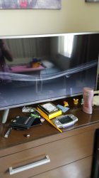
Remember this?
bent-motherboard-goner-jpg.30158

Haha...me too. I have 7 now! This one came in the mail this week:
It looked pristine in the listing. That happened in shipping! Too bad too, cuz this one was factory sealed and a prime candidate for reballing. I still haven't broken the seal to see how extensive the damage is. Luckily the seller refunded me partially. So I only ended up paying $20 for it. From the corner that broke open, looks like the BluRay drive got smacked hard. The Motherboard is cracked in half too. The console barely fit in the box and there was no protection on the top and bottom. Looks like it took a 30-foot fall strait on that corner. Probably sheared off all kinds of components. I've been putting off opening it.

It takes all the wind out of your sails seeing something like this.

Backstory:
PS3 #6 was listed as a "Red Blinking Light for parts or repair" at $40. From the photos I could see the warranty seal was intact. Firstly it was listed as a CBEH1001, the FCC ID, not the model number. That told me the seller didn't know much about what they had and probably didn't know the difference between an overheating RLOD and the YLOD from a hardware failure. So I jumped on the deal!!!

That's when the United States Postal System went...well...Postal on it! It arrived in the condition you can see from the pic above. The case was thrashed! Plastic bits littered the box like BBs on an Airsoft battlefield. The motherboard and RF shielding were bent/cracked from some huge fall right on the back top corner. The BluRay drive was clearly bent too! After seeing what the USPS had done to my purchase, I didn't even bother opening it. I put the thing back in the box and there it's sat since. Luckily the Seller gave me a $20 refund. As he pointed out, It was listed for parts anyway. It's just a real shame, considering the listing and condition in the photos, It had a really good chance of being a great deal on a console with a high potential for fixing!

After getting PS3#7 working, finally, I figured I'd finally circle back to #6 and see what the real damage is. Sorry no pics. Anyway, the inside was the filthiest console I have seen. The dust was caked on and sticky. In some places had pitted the metal! When I'd take IPA to it, it turned black and tarry. My guess is the console was from a smoking household. What a filthy habit! It was a PITA to cleanup.

The BluRay was bent in half, but luckily it was only the back corner and when I opened it up the plastic was fine. Only the RF shielding was bent. So I just had to pound it out strait again. No problem there. It was of course dirty, so I took the opportunity to clean it thoroughly.

The RF shileding and MB were bent at about a 30-Degree angle in that corner with the HDMI encoder and 1000uF caps that attenuate the AV signals. In fact the force had popped one of the 1000uF caps off the board and it fell out! It looked like a clean break and tested fine, so I just soldered it back on. I bent the MB back to about 5-Degrees. I didn't want to go too far and make it strait. I was afraid of bending the layers too much. If they hadn't already been destroyed, bending it back could do it. I just wanted to get it close enough to straiten the RF shield and close the case again. So 5-degrees was enough. I didn't want to deal with deliding yet and didn't see any other obvious damage, so I moved on.

The power supply was a ZSS (the first one I've come across). I actually like the design of it better than the APS-226. I know they are less efficient, run hotter, and are thus less reliable. However, it has a copper heatsink for the regulators that contacts the aluminum RF shield with a thermal pad that's got a TIC coating. And it's screwed together for good contact. The APS-226 only has screws on the sides, non on the top to use the RF shield as an additional Heat Sink. Cool design. Too bad it's needed because of inefficiency. It's a cleaver design that would have helped the APS-226 last longer had they done the same. Anyway, it badly needed a cleaning as it was packed full of dust bunnies. I thoroughly cleaned it and inspected for shorts and scorch marks. It looked fine. I added some MX-4 to the heatsinks to make better contact with the RF shield during reassembly. It's good to go now, assuming it would work. Again, I didn't know until I could conduct a PWR test.

The WIFI antenna was cut off! When the BluRay drive was smashed by the fall it slammed into the Power supply and the WIFI antenna cord that runs between them was cut cleanly by a bent piece of RF shiled. I had a replacement from the Carcass of PS3#1, who's motherboard was sacrificed as payment to my reballing education. So now PS3#1 has save the life of PS3#7 with it's inductors and PS3#6 with it's WiFi antenna! Well, assuming this isn't all for nothing. Given the damage to the motherboard, it's a longshot (at best) that this thing is salvageable. That's to be determined. Regardless, PS3#1's sacrifice hasn't been in vane - which that feels cathartic, in an organ donor kinda way.

I reassembled the console after pounding the RF shield strait. Everything actually looked like it might work. I guess the first PWR on will succeed or fail based on how badly the bent motherboard was damaged. So I plugged it in and gave it a test.

...Green light (so far so good)...
...no beeps (I am Shocked!!!)...
....no video via HDMI (Okay, maybe it's got a GLOD)...
...Plug in a controller via USB and got it to pair (not a bad GLOD)...
...Plugged in an AV cable to my CRT and got a the screen saying a 'HDMI device was found, do you want to switch to it?' (WOO HOO!)...
...I press okay for it to switch to HDMI and...

...Nothing! (Dammit!)...
...the fan started ramping up to maximum now and the Yellow LED started flashing, so it was time to shut down - it's overheating. End of the PWR test!

Okay, so the HDMI doesn't work but the AV does? I did notice alot of audio noise coming from the AV cable. I wiggled the cord and it kinda helped, but didn't get rid of it. So I started to worry that maybe the traces in the internal layers of the PCB near the HDMI encoder got affected. I mean, it's near the corner that got bent! It could explain a GLOD, but why would the AV still work? And why no YLOD HDMI error? The AV wasn't really working well. The audio interference was pretty bad. I looked up what those 1000uF caps do and they attenuate the AV signals (YPbPr composite, etc). So it seemed like a likely place to start. Maybe they were damaged.

So I disassembled it again and tested the ESR with an ESR meter. This is what they are designed for (aluminum electrolytics). They all tested fine compared to the carcass of PS3#1. I went ahead and touched up the solder on all of them just in case.

I took the opportunity to delid and as I suspected, the CPU was overheating. There was no TIC anymore, it was completely shiny. The RSX had great TIC contact though. So I actually had a console where the RSX was cooling fine, but the CPU was overheating and it was full of dust. Basically that means the RLOD was just a CPU overheat, which actually protected the GPU from thermal cycles that could have destroyed it's BGA. So that's probably what saved the RSX's BGA!

But what about the HDMI? I still didn't have an explanation for why it didn't work. So I had a closer look at the HDMI port and the problem was apparent. In my haste to find a problem on the motherboard and having my attention on the bent corner, I competently forgot to look at the port itself. It was mangled. The plastic bit, that's supposed to be in the middle bracing the pis, was missing!
iu


Uh...well that might explain why I didn't get an HDMI signal! The damn port is busted..lol! So I had to perform my first HDMI port swap. It went. I had trouble getting it hot enough thanks to the PS3's 6 layer design and redicuolus ground planes. So I had to resort to usign the board preheater. I covered everything in aluminum foil except the HDMI port, like a surgeon prepping the area he's about to cut. That was to reduce warping from the cool air above the board making a large temperature differential. Then using amtech flux and fresh 60/40 solder I was able to get the joints to wet well and using hot air it came out just fine. This is where PS3#1 is the donor board that keep donating. It's HDMI port went in like a champ. I let the board cool slowly to prevent warping and hopefully stave off any BGA damage. I was really not wanting to put it on the preheater because there is a high chance of popping a BGA from the stress. So I was careful with the foil and heatup/cooldown cycles to minimize warping. It seemed to work. The board came out as strait as it went in (except for the corner the USPS origami'd).

And the result?
Much to my befuddlement, I actually works! I tested it for an hour this morning and it plays fine. Everything just works now. Freaking unbelievable!!! I still can't believe it. A $20 CECHA01 that was almost certainly trash. I wrote it off for months and it pulled through like the freaking Black Knight...
holy-grail-1.gif


So another one survives the United States Postal System!
 
Last edited:
@RIP-Felix Good points. And I frequently forget to check fuses until I've been pulling my hair out for hours, so.... yeah.

Low melt alloys are great for those thick lead free boards that are just giant copper heatsinks. And for keeping temperatures safe and low on bigass 200 pin QFP chips.

Not only are these jigs to prevent warping during rework, they're great for baking out warp: https://www.aliexpress.com/item/32852109892.html
 
I'm new here and been following this post for some time, all you guys have done some fantastic work on this, so I figured I would finally look at my RLOD PlayStation.

Last summer I picked up a PS3 CECHE01 at the Flea Market for $10, it's never been opened. It'll RLOD in 2 seconds.

When I took it apart to clean all the dust out of it, I noticed this unit got really hot, so much so that the plastic around the fan deformed. Also the outer plastic of the PlayStation is a little deformed from excessive heat. I'm kind of wondering if the fan doesn't work anymore? The fan doesn't seem to turn on, but then maybe with the unit turning off in 2 seconds, it doesn't have time to even start up?

So today I had some free time, and decided to try the Syscon Error Reader version 0.4 on it, I used the new version that doesn't require Python to be installed, it was very simple to use, you guys amaze me with what you are all doing, again, great job to all of you, it's been a fun learning experience for me.

So attached I have the results from my test, does this error look fixable?

Dang it, I can't upload the image..., well the 20 errors are all the same, they are....

00000000 A0003001 FFFFFFFF


An update on my PS3, I tried a different power supply, this one does solve my 3001 error. The PS3 now RLOD around 4 seconds, and the fan now kicks on! So my original power supply did have issues.

So with the 1st problem solved these are the next two that are showing up, numerous times turning on the PS3 these two errors keep alternating on the list,

00000000 A0404402 FFFFFFFF
00000000 A0403034 FFFFFFFF

which looks like a BGA connection issue. So now I'm stuck unless I can get it reballed someplace, I looked around locally and haven't had any luck so far.
 
A few spreadsheet updates. Forgot to get the info off of the warranty return, suck it.

@RIP-Felix I was just cleaning up the shop and found a little ziploc baggie with all of the extra parts for my scopes / probes.... including ground springs. Sigh.
 
A few spreadsheet updates. Forgot to get the info off of the warranty return, suck it.

@RIP-Felix I was just cleaning up the shop and found a little ziploc baggie with all of the extra parts for my scopes / probes.... including ground springs. Sigh.
You mean the warranty for the USPS damage to PS3#7? Also, did you ever get to PS3#4 (the one I traded you for PS3#7)? It should have been a prime reball candidate. I'm just curious if you were able to make out good on your end of the trade.

Glad you found them accessories, they're useful...and easy to loose!

Something of note, from my experiments with the tokins/tantalums, is that the YLOD and 1002 errors continued after the "Bad waveform" disappeared and we would normally consider the noise acceptable. So there is a noise threshold that causes YLOD, but that would probably pass undetected by our O-scope methods.
  • RSX Array: 4 Tokins - 0 TaPol (270uF) = Non-Instant (2-10s) YLOD, 121mVpp Bad Tokin Waveform, 801002 Syscon error
    Startup Seq. (HiRes Acq.).png
    RSX Bad Tokin Noise (DC Coupling & 1x probe).png
  • RSX Array: 0 Tokins - 4 TaPol (270uF) = Random (Normal Stress) YLOD, 30mVpp Good Tokin Waveform, 801002 Syscon error.
    O-Scope, L6202 Replaced + 4x TaPol Arrays on RSX (Startup Seq. less noise, more stable).png
    O-Scope, L6202 Replaced + 4x TaPol Arrays on RSX (Much less noise, noticably more stable).png
    O-Scope, L6202 Replaced + 4x arrays + Parasite (Clock signal maybe).png
  • RSX Array: 0 Tokins - 4 TaPol (470uF) = Working, 10mVpp Good Tokin Waveforms.
    Working Startup Sequence.png
    Working Target Plateau.png
    Working 60Hz Signal.png
So there was really no way to tell. The only way I saw was possible was the noise in the 60Hz signal was obviously lower. I think that was because the HF noise component was better handled by the 470uF caps than the 270uF caps did. Tokins have an advantage there. So it's clear when the tokins are bad (bad waveform). It's not so easy to be sure the tokins are good, just from an oscilloscope measurement. Testing for stability and SYSCON errors is still necessary.
 
Last edited:
I've bought a faulty warranty sealed CECHA06 that shows the YLOD about 1 second after pressing the power button obviously then I get the 3 beeps and blinking red led.

Q1. Does this sound like a candidate for the tokin cap replacement?

Before I remove them can someone tell me how to heat them up for testing to see if I can revive them and see if the PS3 will boot.

Q2. At what degrees and for how long?

I've also seen someone say it might be too quick and to check the cpu/gpu voltages.

Q3. How would I go about doing that?

Q4. Also is replacing 1 tokin cap one side with 4x 470µF caps enough to carry the load of say the matching cap the other side of the motherboard if it was faulty as well?
 
Last edited:
Back
Top