Pacorretaco
Member
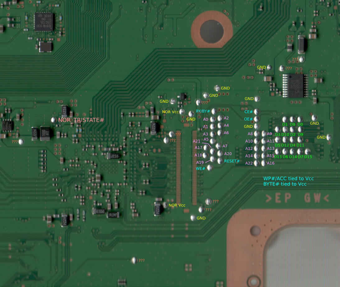
Haha, could you show us that video? I'm curious. Probably it was a friend of mine hahaha.I saw a video where only TX and RX were needed (I think, I might be wrong). Always I read the pdf I don't understand where to connect the GND.
I'm using Windows 10 with python27, ft232r usb uart
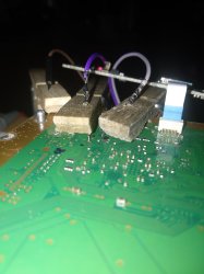
I couldn't solder where it says the GND in the motherboard, should I use a knife to scratch it?
So I though well when I saw something like receiving the command after sending it
All devices need to share the same GND in order to communicate. If you are not using the GND wire and you are having problems, the first thing you need to try is connect proper GND. A simple alligator clip will be great.
And yes, sometimes it can look like it's working without GND, but it's going to be less reliable or it's because all grounds are already connected together via earth wire.
You can get GND from pretty much anywhere on the machine. An alligator clip is perfect for this. Or you can just get creative. The connection doesn't have to be so strong.I couldn't solder where it says the GND in the motherboard, should I use a knife to scratch it?
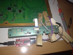
In fact your soldering with rigid pins to the board looks scary. Be careful really not to break the pads. (It wouldn't be the end of the world, but yeah take care)
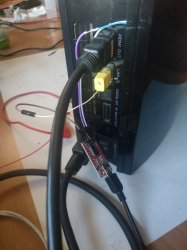
Edit: (Normally I like to get ground from the ethernet port, when the machine is assembled. I just jam a wire in there with the ethernet cable. Just an example)
Attachments
Last edited:
")
 . You could attempt a reflow, although a reball is better.