PS3 Frankenstein PHAT PS3: CECHA with 40nm RSX

@sandungas I was personally thinking of intercepted the spi when seen only 3 wires are soldered on those modchip, +2 of power line which could be 1.8v?
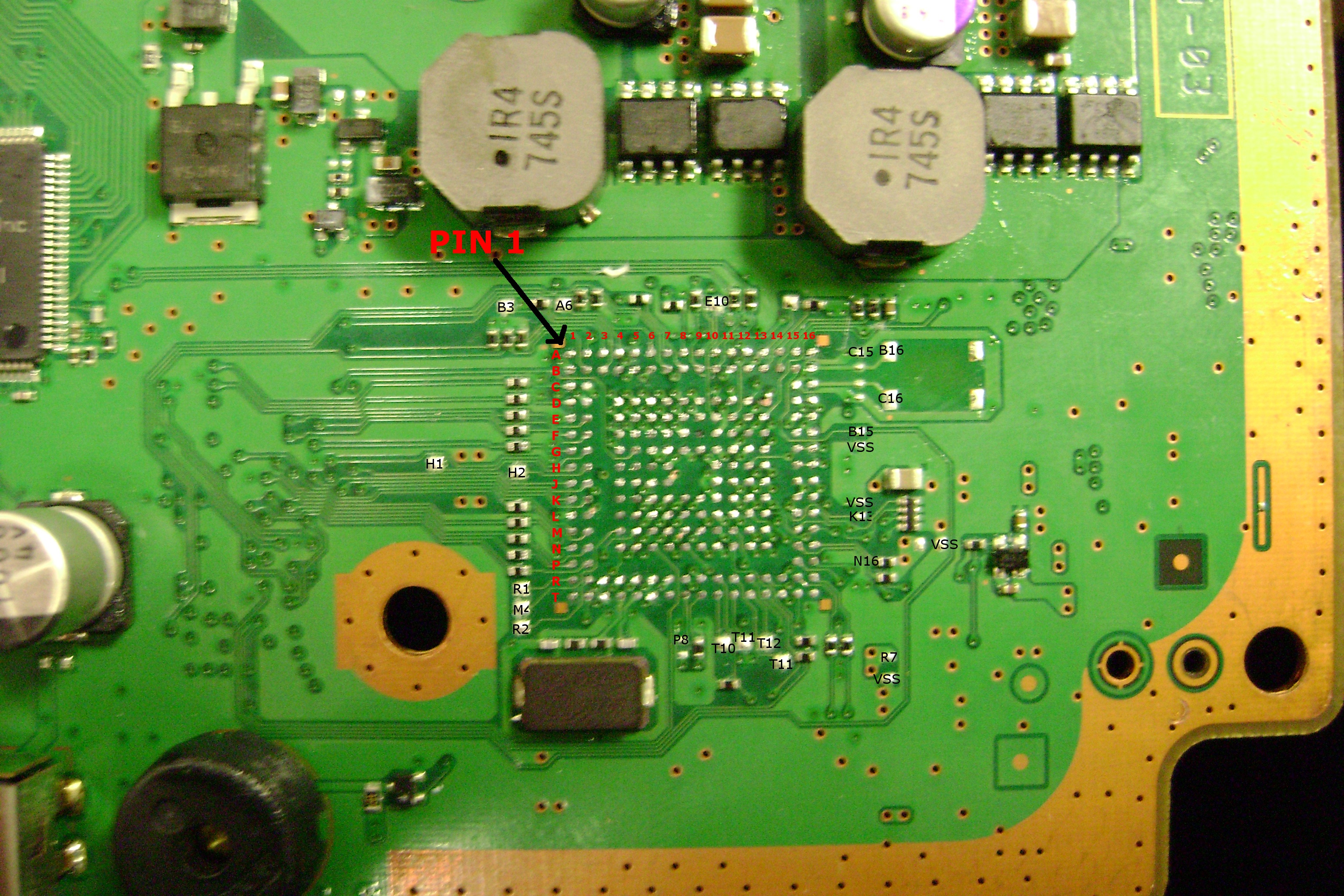
Where the idea with decap memory coming, knowing ram pinout and excluded from rsx pinout then rest will be in and out to AV/hdmi ic. A reverse engineer to rsx would help to understand what each unit does in heat panic /bad connection to mobo.
 
@vyktormvmpay25 Nah I understood you perfectly that you were referring to the 4000 series with the 40nm. But now that the cat is out of the bag and the 28 nm is being discussed given that the pcb for the 3000 and the 4000s can support the same 40 nm rsx would it be reasonable to infer that the pinout for the rsx should still be the same?

@DoublesAdvocate
Onto your points youre absolutely right we don't know for sure that the 28 nm is more reliable. But we can say with full confidence it is more power efficient and it was the final revision of the rsx that was used in consumer models(nobody knows for sure what sonys psn ps3 servers use nm wise. Probably the last revisions). Further as the youngest rsx units produced they have the edge of being the newest of the old stock. And while you're right we can't be confidant that the firmware would play nice with the 28nm it's important to remember until these frankenstein units came into the forums eyes we didn't even know this was a thing that sony was doing.

My rambling point here is that the 40nm on the 4000 may need a replacement ihs to be used and if that's the case we might as well consider if the 28nm is theoretically possible. After all between its increased power efficiency and the massive heatsinks of the original ps3 models it might be possible to safely run the systems on stock firmware.
 
Last edited:
I guess the modchip could be using 3.3v (like syscon), but well... this is going to be easy to find, probably Xilinx manufacturer have the datasheet available. The tricky thing is that is needed to sniff the SPI bus 2 times in the same console to compare them:
1) with factory RSX
2) with modchip + new RSX

Or...
1) at the syscon pins (before the mochip modifyes SPI communications)
2) at the RSX pins (after the modchip modifyes SPI communications)

This comparison is going to tell us where is "the magic"
And "that magic" is our goal, we need to see if is posible to build a custom syscon patch to achieve it (still doubtful)
 
Last edited:
@Squiglemouse yes they have same pinout. Well I will try to get in touch for the modchip. One should be enough for experimental tests.
4ab0711e51339dfb8816259c38144ba7.jpg

CPU is dead and good rsx went to another motherboard. Funny thing this cpu is with white silicone like 2100/2500 but can not be delided, nobody should try to delid white silicone. Is soldered on ihs I think. Only grey silicone models can be delided for most 2503 models.
 
Last edited:
If my order succeeds, I can send the second modchip to whomever wants it for experiments ( though can't cover shipping prices since I'm a broke student).
 
Here are the boards each of those pictures is from.
COK-001/2 I couldn't find a picture of this that wasn't a photo of a photo.
COK-00.jpg
IMG-20210312-WA0017.jpg


VER-00X
VER-00.jpg

DYN-00X
DYN-00.jpg

DIA-00X
DIA-00.jpg

SEM-00X
SEM-00.jpg

edit: added 2nd COK-00X installation diagram to this post as well.
 
Last edited:
One other thing that may be useful for not only this but also potentially other diagnostics and repair is this e-book I found when looking up this stuff. I think it's all in Indonesian so @feel2death might be able to tell us if it has anything related to this, or just anything useful in general.
https://ps5on.blogspot.com/2017/10/ebook-service-all-playstation.html

its aint useful i guess its like common problem and already found from here like how to unbanned ps3 etc
 
We have schematics we find it with time which pin is used.
We can deduce them for all motherboard models with a syscon from the CXR series
https://www.psdevwiki.com/ps3/CXR713120-201GB

The modchip is taking ground from a corner (there is a big solder blob in the corner in all images), and the other wire "alone" is volts
And the SPI data communication is made with 3 "wires":
RSX_SPI_CLK (solder pad G1)
RSX_SPI_DO (solder pad F2)
RSX_SPI_DI (solder pad F1)

The names of the solder pads are in this image from wiki... is needed to remove syscon to see where goes each, but well... as far i remember there are some photos in wiki, and maybe some of you have a motherboard with syscon removed to take a photo of the solder pads and traces
q0jJbJv.jpg


----------------------------
Sadly, we dont have that RSX SPI pins mapped in the syscons from the SW series :/
https://www.psdevwiki.com/ps3/SW2-303
But im guessing the protocol is identical... some of the photos posted by @DoublesAdvocate belongs to motherboards with syscons of the SW series, and it seems the indonesian modchip is dealing with them without any problem... most probably because is doing exactly the same in all them
 
Last edited:
...But now that the cat is out of the bag and the 28 nm is being discussed given that the pcb for the 3000 and the 4000s can support the same 40 nm rsx would it be reasonable to infer that the pinout for the rsx should still be the same?
Is it though? It was my understanding that the 28nm RSX wasn't pin compatible with the 90-40nm RSX. If they are, then wasn't there a FW or SYCON reson that we couldn't select it? And if it is pin compatible, but not possible in FW/SYSCON to enable it, then maybe a SPI spoofing MOD CHIP could? Is that what you're getting at?
 
Is it though? It was my understanding that the 28nm RSX wasn't pin compatible with the 90-40nm RSX. If they are, then wasn't there a FW or SYCON reson that we couldn't select it? And if it is pin compatible, but not possible in FW/SYSCON to enable it, then maybe a SPI spoofing MOD CHIP could? Is that what you're getting at?
I don't think anyone's fully tested it yet so that's part of the problem.
Oh, I was also able to find another picture of a COK-001 with what looks like an RSX mod from back in 2018 on Indonesian facebook.
46398216_2360786820617253_8649477377186856960_o.jpg
 
Btw, the photos posted by @DoublesAdvocate is a proof that the modchip allows to use a 40nm RSX (first time introduced in the PS3 slim models CECH-21xx) in the previous slim model CECH-20xx with motherboard DYN-001 originally with a RSX of 65nm
Also, same stuff for the last version of the fat motherboards VER-001 (PS3 models CECHL, CECHM, CECHP, CECHQ)

Both motherboards DYN-001 and VER-001 with a syscon of the SW series
 
Huh...that would be awesome if we could pair a 28nm to the A/B models. My gut tells me that the PWR distribution/filtering was so radically redesigned it wouldn't work. A 40nm is still a more available part, and certainly the heat sink designed for a 90nm is OP for it. Should be great either way!
 
We can deduce them for all motherboard models with a syscon from the CXR series
https://www.psdevwiki.com/ps3/CXR713120-201GB

The modchip is taking ground from a corner (there is a big solder blob in the corner in all images), and the other wire "alone" is volts
And the SPI data communication is made with 3 "wires":
RSX_SPI_CLK (solder pad G1)
RSX_SPI_DO (solder pad F2)
RSX_SPI_DI (solder pad F1)

The names of the solder pads are in this image from wiki... is needed to remove syscon to see where goes each, but well... as far i remember there are some photos in wiki, and maybe some of you have a motherboard with syscon removed to take a photo of the solder pads and traces

I have a COK002 with a syscon removed atm. Do you need pictures?
 
I have a COK002 with a syscon removed atm. Do you need pictures?
Im tempted to try to compare the images availables to try to figure which wire is each by his name (the 3 from the SPI bus). The best thing we could do with that info is to take the images posted by @DoublesAdvocate and paint on top of them the SPI names of each wire
This could help a bit if someone is interested to "sniff" the SPI communications

In wiki there is a photo of a DIA-001 with the syscon removed... is a bit blurry, but i guess this one is good enought
It allows to see where is located each solder pad, we can see where the trace goes to a "via" (hole) and allows to follow it with a multimeter... it should match with the photos of the modchip installations
I noticed the photos of the modchip instalaltions are always soldered to vias... and at an intermediate point of some kind of bigger "data bus"... so most probably the modchip can be installed in any side of the motherboard, keep that in mind because we are not restricted to do the connections exactly like in the photos of the modchip installations ;)
I mean... for every photo of the modchip installation... we can consider there are "alternative" solder points at the other side of the motherboard

Syscon_top.jpg
 
Last edited:
Geez, I log out for a week while in mourning over my car and the world is turned upside down.

I've got more patio drinks on the schedule tonight, then I'll see if I'm sober enough to make a few little changes.

I would ABSOLUTELY pay 10 bucks a pop to not have to swap the syscon and make all those changes. It would save 2 full rework cycles on the board. That's 2 chances for popcorn.
 
I have a COK002 with a syscon removed atm. Do you need pictures?
What you could do is use a multimeter to trace the path of the JTAG to the test pad locations on the motherboard. AFAIK that's not been documented. I suspect they are one of the row of 5/6 pads near the CG reset mod.
Possable JTAG location.png

Isn't there usually a way to test the BGA connections pin-by-pin with the JTAG? Or does SONY obfuscate the protocol in some way that make it impossible to check the health of the daisy chain? Regardless, if we can find the JTAG test pads, it would make programming/dumping the SYSCON easier.

EDIT: Never mind, I was thinking they SYSCON JTAG might be connected in line with the RSX JTAG. SYSCON JTAG is disabled from the factory after production on retail systems. I guess the RSX JTAG would require a JTAGulator to figure out, and then it might only be useful for diagnostics, but probably not since the RSX is a custom chip.
 
Last edited:
Geez, I log out for a week while in mourning over my car and the world is turned upside down.

I've got more patio drinks on the schedule tonight, then I'll see if I'm sober enough to make a few little changes.

I would ABSOLUTELY pay 10 bucks a pop to not have to swap the syscon and make all those changes. It would save 2 full rework cycles on the board. That's 2 chances for popcorn.
Welcome back! The world's changed since you've been gone! DO THIS NOW!!!
cg-reset-png.32000
 
Back
Top