botakompong
Member
the same q6200 form only exists in cok-001 and cok-002When he say COK 001 only,
Maybe he means all 90nm models?
COK 001, COK 002, SEM 001, DIA 001
the same q6200 form only exists in cok-001 and cok-002When he say COK 001 only,
Maybe he means all 90nm models?
COK 001, COK 002, SEM 001, DIA 001
yes, before I named rsx "cxd", I was initially confused with the designation 40nm, 65nm, hahaha, but I was able to follow ...Btw, im going to make a list because i been messing around with this RSX wiki pages latelly, we can group them "by series" and we can consider the "suffix" doesnt matters when talking about the compatibility in between them
The name starts with "CXD", then this numbers, and finally the suffix "GB", "AGB", "BGB", etc...
https://www.psdevwiki.com/ps3/Template:Motherboard_Components
RSX 90nm = 2971
RSX 65nm = 2982
RSX 65nm = 2991
RSX 40nm = 5300
RSX 40nm = 5301
RSX 40nm = 5302
RSX 28nm = 5305
Just incase you can choose, try to get the newest number (except 28nm that is not phisically compatible with the solder pads of older RSX models)
No problem, i was thinking in it and decided to make the list because the names could be a bit confusing, but also because what you mentioned about the voltagesyes, before I named rsx "cxd", I was initially confused with the designation 40nm, 65nm, hahaha, but I was able to follow ...
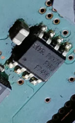
By the way, here is picture of the official SONY 65nm COK 002 Frankenstein v1No problem, i was thinking in it and decided to make the list because the names could be a bit confusing, but also because what you mentioned about the voltages
I guess the motherboards that had the 90nm from factory are the ones that are feeding RSX at 1.2v
And i guess the 40nm RSX models are the ones that works at 0.95v
And the 65nm ones... i dont know
I will wait for @RIP-Felix review of the voltage reduction mod you suggested (im sure he is not going to let that fish to escape, lol)
And i guess at some point some of the people that is using this mod is going to need to check that voltages in different RSX models and motherboards

I'm guessing IC6200 was changed to allow the manual setting of voltage to 0.95v by populating R6214 and R6216 with the appropriate values as calculated using the equation quote above. RAM can usually accommodate a range of voltages. Heat and electromigration are the consequences of voltages near the high end of the range, but stability can suffer if you push it too low. Whereas the 90nm RSX needed the higher voltage to remain stable, my guess is that the smaller 40nm manufacturing process allowed them to lower the voltage without stability suffering, as one would expect. That jives with what I know about overclocking processors/RAM in general, so it makes sense. I was wondering if this info would pop up again and why these changes were made on that console..lol. So I guess now we know!And a few latest thoughts about the added resistors.
Based on this picture, it's very difficult to tell how many resistors and/or if the whole IC were all replaced.
View attachment 29570
However, having looked at the schematics a bit more I may have a better idea of what happened in that particular PCB neighborhood. But please remember, I am only speculating.
What they did was most likely install another IC - BD3504FVM (Or something similar to it) instead of the BD3520FVM. Why? Possible reasons could be that the original was faulty? Maybe it was causing 1.2v VDDR line to be unstable? Was it just a precaution?
Another potential reason is that BD3520FVM is only meant to output 1.2v, however the 3504 model can be adjusted to give out variable (0.65~2.5V)...It is probably still set up to output 1.2v in the circuit (I'm assuming?). Or is it possible that the new voltage might actually have been changed entirely? Have there been changes to RSX voltage in further revisions?
Anyways, the IC and around 2-4 resistors were most likely added/replaced to accomplish the same result as what the original BD3520FVM was doing. Why extra resistors? Because BD3520FVM already has them integrated into the IC, while BD3504FVM does not. This IC allows engineers to manually configure required output voltage for the application.
Once again, if my theory is true, these are the only differences. What does it mean? Well, there may be no immediate need to mess with this particular IC. Or you can recalculate the needed values and do it similarly to provide 1.2v (or something higher/lower) . As it stands, we don't have enough information why it was done or what voltage it's actually providing
Here are some pictures to illustrate what I'm talking about. Notice the logic around IC6200
View attachment 29571
Now here are very similar ICs used in DC-DC converters on the next page. Look at IC6303 (in red), notice the similarity to VRM for RSX ? Notice further, IC6602 (in blue) is doing similar job as the one in red, but with extra resistors, as they are not originally inside the IC, but we still need to use them to get 1.2v
View attachment 29572
Resistors inside BD3520FVM, hence no need to install R1612 and R1614. IC output is already designed to be 1.2v.
View attachment 29573
And here you get to choose your own resistors.
View attachment 29574
The formula for this is luckily inside the datasheet:
View attachment 29576
Let's test the equation with the example of IC6602 and its resistors . R1 is equal to R6606, which is equal to 3900 ohms. Therfore R1= 3900 ohms. R2 in this case would be equal to R6607 + R6609 (dont be confused by double resistors, it was probably done to achieve needed value), so 3300+470 =3770 ohms. R2 = 3770, Now plug these numbers into the formula to calculate Vfb terminal to see what happens. Vout will be 1.2v. So we are finding Vfb. The equation is 1.2=x* ( (3900+3740)/3900), x=0.612 v. Fbd is going to be 0.612v this way. As the text states, Typically Vbd is controlled to achieve 0.65v, so this is close enough..So the formula is true. (side thought: you could actually get perfect 0.65v on Vfb if you drop the 470 ohm resistor and use only 3300 and 3900 ohms as the datasheet suggests. Now I don't know why it was designed to get it down to 0.61v, but Sony engineers probably had a reason). And you could also adjust the output to be different. Remember, anywhere from 0.65 to 2.5v...
Now I apologize for terribly long text , but this might clear things up a bit. So what resistors to replace and which ones to add you may ask? If you plan to keep 1.2.v in that line, I will add that info a bit later as I honestly have been spending too much time on the research...
Man I just love the way you dive deep into these research subjects and share your results with the community. IIRC @botakompong stated it was kinda optional.. When I get the proper tools and experience I might try it on my beloved A01 in case its RSX failsOn the COK-001 schematic (3rd ed.), Q6200 is a Si4866DY N-Channel Reduced Q, Fast Switching MOSFET. It's driven by IC6200, an N-Channel MOSFET driver. This is similar to how the other voltages are delivered to the RSX. Q6200 feeds 1.2v_VDDR. R is RAM. Interestingly, on my COK-001 I have what looks like the same Q6200 that picture @Pacorretaco posted from the 65nm SONY Refurbishment COK-002 (an IRF7456). Interesting that the schematic and actual parts on boards differ, but they must be interchangeable. Perhaps it went EOL...IDK.
So this goes back to an older question we had about the compatibility of voltages between generations of the RSX. A while back I wondered if the voltages were all the same or not? After looking at the datasheets for the various RAM modules (or the closest schematic we could find), the voltages were all within the same general range and should work fine. In one of the SONY refirbished consoles (not sure which off the top of my head) @DeadEnd noticed a few of changes made to resistors R6214 and R6216 on IC6200...
I'm guessing IC6200 was changed to allow the manual setting of voltage to 0.95v by populating R6214 and R6214 with the appropriate values as calculated using the equation quote above. RAM can usually accommodate a range of voltages. Heat and electromigration are the consequences of voltages near the high end of the range, but stability can suffer if you push it too low. Whereas the 90nm RSX needed the higher voltage to remain stable, my guess is that the smaller 40nm manufacturing process allowed them to lower the voltage without stability suffering, as one would expect. That jives with what I know about overclocking processors/RAM in general, so it makes sense. I was wondering if this info would pop up again and why these changes were made on that console..lol. So I guess now we know!


Now there may be more than one way to skin this cat, either by replacing IC6200 (BD-3520 with internal resistors set to 1.2v) with one that allows us to set it manually VIA pads on the motherboard (eg. BD-3504), or by replacing Q6200 with the one @botakompong suggests. This latter solution I don't really get though. I can't tell what it is. I recognize the logo (Microchip Technologies) but the case ID code is meaningless when I search for it. I don't see any current N-ch MOSFETs that shed light on the case code either (usually there is a key to the code in the schematics of similar products, but I couldn't find one that helped). Unless that's not an N-ch MOSFT. IDK, but whatever, if it works, it works!
I'm not sure if that's a necessary change because the memory on a 40nm RSX requires 0.95v, or if it's just a power saving feature. There is the possibility that pumping 1.2v into the ram of a 40nm that was expecting 0.95v causes premature electromigration and death. Obviously, if you can get away with lowering the voltage there is a heat advantage. Less heat means better reliability. So no reason not to. I just don't know it's required. Then again we weren't able to find the exact schematic for the RAM, so IDK for sure.
Hahaha, most things are optional after all.Man I just love the way you dive deep into these research subjects and share your results with the community. IIRC @botakompong stated it was kinda optional.. When I get the proper tools and experience I might try it on my beloved A01 in case its RSX fails


thank you for helping, for cxd2991 (65nm) there is no need for any changes, because the input voltage is 1 volt