Yeh, but that 2.66V is beyond the max voltage accepted by rdram, i tried replacing the regulator (ic6607), but nothing changed, im getting 2.67 volts there.
The datasheet for rdram says the max is 2.5 +/- 0.13, also the datasheet for the regulator says min/max of 2.45 to 2.55, all the other voltages are correct.
Also the service manual says RSX_FBVDDQ is 1.8v, im getting 2v .
EE+GS do share data lines with RSX, so im keeping that on my head.
Anyway im trying to figure out this voltage differences before trying to continue.
I cant help much with RSX, to be honest i never dedicated much time to understand how it works, neither EEGS
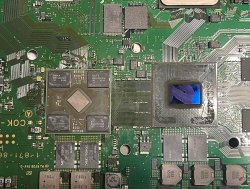
Is just there has been some talks in wiki latelly related with the PS2 "netemu" software emulator that are indirectly related with the PS2 bridge chip (we dont understand well whats its function). And for me this chip was always a mistery so i decided to make the pinout table in wiki, this is when i realized it have 8 pads named "SW" that are related with the EEGS and RDRAM power lines
The reason why this surprised me a bit is because usually most/all power lines are switched directly (or indirectly) by syscon, but in this case it looks like the PS2 bridge is switching the power lines of EEGS and RDRAM, so if we had to draw a graphic of the hierarchy it seems the PS2 bridge is the boss of EEGS
I think this detail is very important for troubleshooting because it would mean that any problem in the PS2 bridge is going to keep one or more of the EEGS subcircuits unpowered
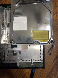
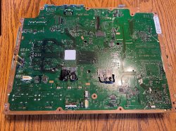
I didn't include the PS2 subsystem's power on that flowchart. I do have one in which I colored in those areas, but the test pads are all on Side B anyway. People are used to looking at the side of the boad with the chips, but SONY designed it to be tested with flying probs on side B. Which works better anyway because we can leave the fan on. I have a testpad location chart
here.
I was looking at your image yesterday trying to figure how to draw that lines and it seems are going to fit fine
")
If you make another version of the image please keep the same exact size in pixels and replace it in wiki in its page where it tells "upload a new version of this file"
Btw, im not completly sure if the PS2 bridge is either switching the mitsumis responsibles to generate the power lines of EEGS and RDRAM... or if is just monitoring that ON/OFF line of the mitsumis
My confussion is because if you take a look at the service manual, all the PS2 bridge pads named "SW" are labeled with an "arrow in" (indicating that are PS2 bridge inputs), and are connected to the voltage regulators (the mitsumis)
But in the voltage regulators (mitsumis) are also labeled with "arrow in" (indicating that are the control signals that switches them)
So... if we trust the arows of the schematics... who the hell is sending the "output" signals in that lines ?
At this point i think the "arrows in" of the SW pads of the PS2 bridge are a mistake in the service manual (are outputs, not inputs), what do you guys think ?
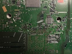
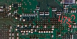
Looking on the schematics page 27 ic 7001 pin 13 is tapped to EE enable(w1) and GS enable (w2), but also tapped to the ground, that's too complex of a circuit for my hobbiest electronics xd
Yeah, following the lines of EEGS pads W1 (EEenable) and W2 (GSenable) to bottom direction are tied to GND
I guess this simply means sony had some prototypes where they was controlling them separatedly by another component, but in retail production they keep them permanently connected to GND (always enabled), i guess in some kind of "idle mode" by default to reduce power consumption
Edit:
Or is a design detail inherited from PS2, just because in some revisions of the PS2 motherboard the "EEenable" and "GSenable" signals was controlled separatedly
Anyway... it doesnt have any importance, are not related with IC7001

 never had problems with it I guess I will wait price go down on these mods if it's compatible with DECHA00A I always find someone selling these dead already