PS3 Help with CELL remarry (and RSX Orbis mod)

PSXCON22

Forum Noob
Hey there,

I need some help with a project of mine because i'm a little bit exceed.... Hope that you would provide some good tips ^^

It's been a while that i follow this thread: https://www.psx-place.com/threads/f...syscon-first-steps-and-error-reporting.30100/, because i've an old PS3 (CECHC04 Pal) that have done an YLOD (back in 2013) and younger me tryed to repair it by himself.... big mistake

Unfortunably, i've scratched the substrate of the CELL CPU during the process (during a delid).

jud6.jpg


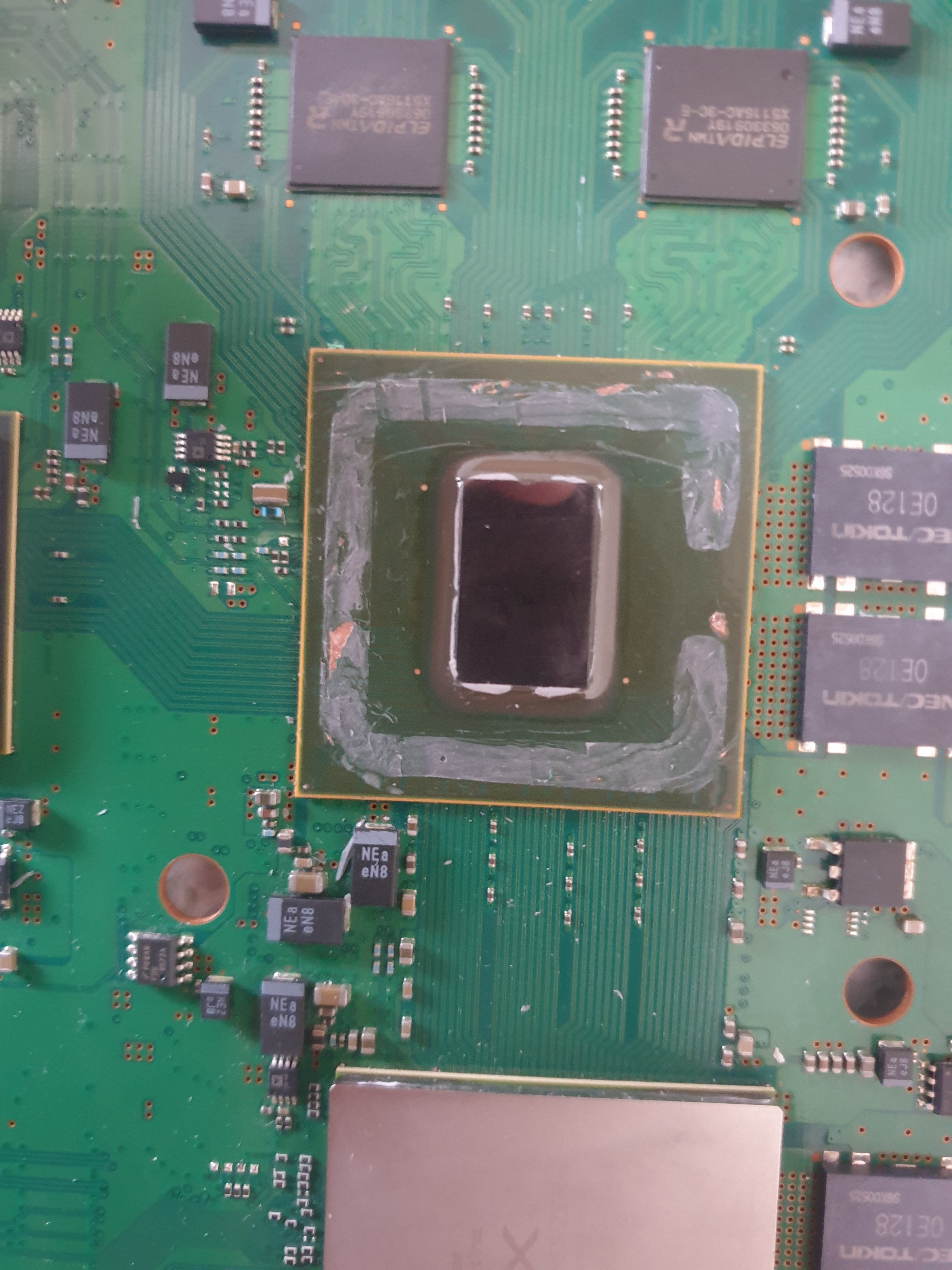
Luckily i've not trashed it away and kept it up to this day.

So, since i have a better comprehension of electronics now, i've dedicated my past few week to try to repair my old friend.

I followed all the tips presented in this 3 videos:

Bought an UART chip, setup my computer and prepared the motherboard for this task :

zbhu.jpeg


I sucessfully accessed the errlog of my syscon :

wez6.jpeg


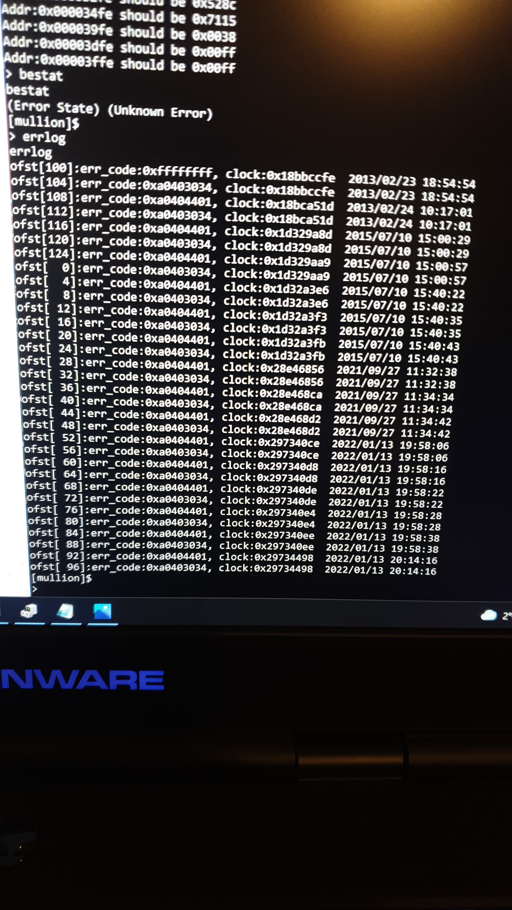
So the Errlog show us the classic 3034 error (poor BGA connections with the RSX)

So, with the help of a BGA Professional ( https://www.ebay.fr/usr/kotom90?ul_noapp=true ), I will perform a 40 nm swap (with an Orbis modchip) to make a durable repair on this machine:

https://shopee.co.id/IC-MOD-RSX-i.4565788.3505669213


But it's not the subject of this topic (however, you welcome if you want to share your experience with this mod ^^)

Before make any physical repair onto the RSX, i need to swap the CELL CPU....

And before that, i want to perform some test with Syscon remarry.

I saw here that it was possible : https://www.psdevwiki.com/ps3/Remarry_Syscon

As i unterstood from this topic, i need to:

- 1) Acess the SNVS part of the syscon eeprom, blank the bytes, between 0x0000 and 0x2800, with FF

- 2) write onto the first 48 bytes a magic keys that should allows the Syscon to be put in status 01 and inizialise a remarry.

- 3) Put a byte 00 onto the offset 48C07 that will allow a non secure product mode

- 4) Restart a multiple time the PS3.

- 5) Update the firmware (i'm also not quite sure how to perform this one too)

And with all of that, it wil be good to go .....

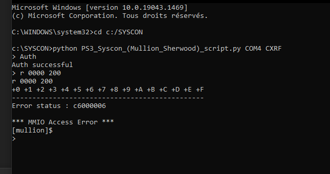
But, and it is the main concern of this topic, i can't acess the SNVS region....

z7al.png


I know that it's related to a master key that need to be put somewhere (because of the SNVS encryption):

https://www.psdevwiki.com/ps3/Keys#SNVS_Keys

But don't know where and don't know how :/ ......

Did the magic key need to be written/enter like that ? :

w 30 A0 96 31 B4 F8 AF C7 77 80 CB 6C 9E EB 08 70 FC

Or else?

Did it need a patch? :

https://www.psx-place.com/threads/syscon-fan-settings-coordinate-graphs.31188/page-4

On step 2 did i need to rewrite the first 48 bytes like this: "w 0 5E B4 F7 C9 50 62 F1 B2 EC F7 EE 1A 3C E3 D8 D0 C5 C2 73 4B A4 13 3D 2C 9E EE 88 ED 0C A8 15 C7 8F 59 DC E4 35 A8 11 BD 8B EC 4E 95 09 F1 E7 38" ?

On step 3 did i need to also modify the byte 48D8E ? with this key : "w 48D8E 52 79 6F 74 61 72 6F 20 69 73 20 63 75 74 65 21" ?

https://www.psx-place.com/threads/ps3-syscon-mode_auth_data-info.30980/

All your answer will be welcome ^^ i don't know what to do and don't want to make an other mistake ^^

Additional Informations:

My PS3 : CECHC04 - Mainboard COK-002 - Syscon Version 1.1.3_k1 - Syscon chip : CXR713 (So SNVS on 0x0000 -> 0x2800 and NVS on 0x2C00 -> 0x7400)

CELL CPU: CXD2964AGB ( The replacement chip : https://www.ebay.fr/itm/402855339914?hash=item5dcc0ca78a:g:NHoAAOSwGZBgnzxx )

Thx in advance for your help ^^

(Sorry for my english, i'm not as fluent as i want to)
 
I'm not an expert on this dark side of the PS3 scene, but I'm pretty sure if the CELL is dead, you can't do anything about it. Relevant keys for the Syscon are inside the CELL, and if the CELL is dead, then you can't do much about it. It would be different if CELL/Syscon/NANDs where in good state, but this isn't the case. I recommend you to buy a used CECHC/E and perform on it that 40nm RSX replacement. It would be easier and less life demanding..

Oh, and if other want to add their opinion, I can summon some wizards. Pray for their arrive.

@sandungas @vyktormvmpay25 @RIP-Felix @DeadEnd
 
I think it would be easier to do a chipset swap (cell, syscon, nand), but at that point you're better off just using the other MB.

If you want to remarry the cell as an acedemic or passion project, cool. But Its more trouble than it's worth IMO.

You do you tho!
 
I think it would be easier to do a chipset swap (cell, syscon, nand), but at that point you're better off just using the other MB.

You do you tho!

Exactly. None of this extra trouble makes sense. You can find an untouched YLOD CECHC04 in EU somewhat easily. That's going to be way easier because the swap is already difficult enough. As for syscon remarry, it's best to ask @M4j0r about the procedure.

All I can add is that I've made a correction video regarding the resistors and also recommendations about the "proper" way of modifying voltage. The first video did not go into details about the logic behind the modifications, rather blindly copied what was provided to us by the person who makes the orbis chip. But later on with the extensive research from @RIP-Felix as well as many others, we have learned quite a bit more. Sadly, I can suspect that lots of people will not care to read the comments and will take that one video as gospel...

https://www.youtube.com/playlist?list=PLxEtwWDJCoaI5-pci9K9Rs8i4D9S2lYK7


Last edited:
I'm sorry I did not read all this cell remarry process. Reball any ic comes easy for me but on software/programming side I'm limited and it takes me time to understand well before processing anything new. Not say isn't possible but you need multiple boards around to see different tests. One board isn't enough to work with, for easy find parts to harvest.
About writing address and keys I'll suggest wait sandungas or M4j0r reply.
We may probably need step by step tutorial, collect info from different posts /links is confusing enough even for me.
First if you really want to fix it focus on cell side more than rsx as that is easier part (only hardware).
 
The guide says: "The PS3 needs to run a factory (JIG) firmware in order to remarry the Syscon"
The only publicly available one is https://www.psdevwiki.com/ps3/2.43_CEX (JIG).
- 1) Acess the SNVS part of the syscon eeprom, blank the bytes, between 0x0000 and 0x2800, with FF
Yes, but you need to this using the SPI EEPROM interface: https://www.psdevwiki.com/ps3/SC_EEPROM#Dumping_SC_EEPROM_-_hardware_way .
- 2) write onto the first 48 bytes a magic keys that should allows the Syscon to be put in status 01 and inizialise a remarry.
That's right.
- 3) Put a byte 00 onto the offset 48C07 that will allow a non secure product mode
In your case that's setting 0x7207 to 0x00.
- 5) Update the firmware (i'm also not quite sure how to perform this one too)
You need to use the lv2diag.self / manufacturing_updater_for_reset.self .
 
To rephrase what he has told you - remarrying is more work than swapping the whole set (syscon+NAND+Syscon), which in turn is more work than finding another YLOD console that has a good Cell in it and is ready for RSX replacement.
 
I'm not an expert on this dark side of the PS3 scene, but I'm pretty sure if the CELL is dead, you can't do anything about it. Relevant keys for the Syscon are inside the CELL, and if the CELL is dead, then you can't do much about it. It would be different if CELL/Syscon/NANDs where in good state, but this isn't the case. I recommend you to buy a used CECHC/E and perform on it that 40nm RSX replacement. It would be easier and less life demanding..

Oh, and if other want to add their opinion, I can summon some wizards. Pray for their arrive.

@sandungas @vyktormvmpay25 @RIP-Felix @DeadEnd

Hi, thx for your answer ^^,
For this project i'm just interrested to restore this particular model of console because it's a good challenge for me ^^
I've already an other working CECHC04 and a CECH 3004B in my collection but i feel a little guilty that i've damaged this one.
I'm used to restore some old retro-console (snes, gc, ps1, ps2, n64, gba, sdc .......) , but, until now, i'm more famillar with hadware fix than programming ^^
I see that this particular model is a futur classic (such as the GC and the SDC)
So i want to learn new stuff and preserve as much of this console (fat backward compatible ps3) as possible, than simply trash them away^^

(and i'm a little bit stubborn too :') )

PS: your summon seems to have worked^^ thx
 
I think it would be easier to do a chipset swap (cell, syscon, nand), but at that point you're better off just using the other MB.

If you want to remarry the cell as an acedemic or passion project, cool. But Its more trouble than it's worth IMO.

You do you tho!

Hey there^^ (thx for the answer)
as i said to elgris, is a passion project ^^ i already have an other CECHC04 and a CECH3004B but i feel a little bit guilty that i've damaged this one.
And as a retro-console collector and restorer, i want to preserve all the unique console that have a great story (and the PS3 is maybe the greatest of all....)
And that will allow me to learn (or relearn) some new stuff and skill. ^^

( I'm also plan to maybe make a simple tutorial to give some tips and show how to diagnose and perform reparation onto a PS3, but in French )
 
Exactly. None of this extra trouble makes sense. You can find an untouched YLOD CECHC04 in EU somewhat easily. That's going to be way easier because the swap is already difficult enough. As for syscon remarry, it's best to ask @M4j0r about the procedure.

All I can add is that I've made a correction video regarding the resistors and also recommendations about the "proper" way of modifying voltage. The first video did not go into details about the logic behind the modifications, rather blindly copied what was provided to us by the person who makes the orbis chip. But later on with the extensive research from @RIP-Felix as well as many others, we have learned quite a bit more. Sadly, I can suspect that lots of people will not care to read the comments and will take that one video as gospel...

https://www.youtube.com/playlist?list=PLxEtwWDJCoaI5-pci9K9Rs8i4D9S2lYK7


Hi, thank for your answer and if you are the youtuber "Artificial" thanks a lot for your video ! it help me a lot in my project!!

I've seen your comparative video beetween the Frankenstein Mod and the Orbis Mod: you concluded that the orbis mod is easier but the frankenstein is maybe more durable as we don't have much informations about how the Orbis mod work (it tricks the syscon by saying that the 40nm RSX (CXD5300AGB) is a 90 nm moddel (CXD2971AGB) if i'm correct?)
So, if i sucessfully repair my PS3, i think that i will perform the orbis mod (as the franskenstein mod seems more tricky to perform) .
Because the 90nm RSX is based on a NVIDIA chip that is all know to have deffective bumps and underfill...
All nvidia gpu before 2010/2011 (40 nm / 28 nm GTX 5xx and 6xx) have this deffective bumps and underfill. Even nowaday, AMD still use this technologies and have the same problems (nvidia changed his fabrication process) (i learnd that from a BGA Rework expert).
For the modifications that i need to do on the mainboard, i will take a good look at your correctiv video (thx) ^^

v9ax.jpg
 
I'm sorry I did not read all this cell remarry process. Reball any ic comes easy for me but on software/programming side I'm limited and it takes me time to understand well before processing anything new. Not say isn't possible but you need multiple boards around to see different tests. One board isn't enough to work with, for easy find parts to harvest.
About writing address and keys I'll suggest wait sandungas or M4j0r reply.
We may probably need step by step tutorial, collect info from different posts /links is confusing enough even for me.
First if you really want to fix it focus on cell side more than rsx as that is easier part (only hardware).

Hi, thanks for your answer.
You right about spare parts, i thinks that i need to find some donor console such as CECH-3XXX, with deffective hdmi port for exemple, to perform the RSX mod
Unfortunably COK-002 board become pretty rare to find here in France.
But VER-001 and DIA-002 board are much more common and easy to find (but i think that they have too much difference with COK-002 board)
 
The guide says: "The PS3 needs to run a factory (JIG) firmware in order to remarry the Syscon"
The only publicly available one is https://www.psdevwiki.com/ps3/2.43_CEX (JIG).

Yes, but you need to this using the SPI EEPROM interface: https://www.psdevwiki.com/ps3/SC_EEPROM#Dumping_SC_EEPROM_-_hardware_way .

That's right.

In your case that's setting 0x7207 to 0x00.

You need to use the lv2diag.self / manufacturing_updater_for_reset.self .

Hey there, first thing first, many thanks for your answer:

The guide says: "The PS3 needs to run a factory (JIG) firmware in order to remarry the Syscon"
The only publicly available one is https://www.psdevwiki.com/ps3/2.43_CEX (JIG).

So, if i unterstand what you said and shared (sorry i'm a noob ^^ i'm much more familliar with C programming and PC stuff), a JIG is more or less a service mode for the PS3 ? and need to be activate via a command prompt?

And a .PUP files is like a .ROM file (that contains the firmware files for a PC BIOS)?

It contains all the basics settings of the PS3 (based on a linux core?) ?

I've believed that the syscon was programmed with a .bin file into it's own eeprom, and the .pup files, that set all the ps3's firmware stuff, was located in an other NAND chip, am i wrong?

I don't unterstand the link beetween a JIG.PUP and the eeprom of the syscon? for me is 2 distinct stuff.

Is it related to a security stuff?

Do the firmware revision (that is set by the PUP) of the PS3 need to be 2.43 (or so) in order to proceed a syscon modifications?

Yes, but you need to this using the SPI EEPROM interface: https://www.psdevwiki.com/ps3/SC_EEPROM#Dumping_SC_EEPROM_-_hardware_way .

Ok, so i need to purchase other tools for this project >< (it's not a problem either ^^)

Like this one ?: https://www.ebay.fr/itm/143968816874?hash=item218535ceea:g:wJcAAOSwnFJfwMc9
+ https://www.ebay.fr/itm/254189784080?_trkparms=amclksrc=ITM&aid=111001&algo=REC.SEED&ao=1&asc=20160811114148&meid=1985c436fdee400cba7298d804cc2729&pid=100667&rk=1&rkt=3&sd=254189784080&itm=254189784080&pmt=0&noa=1&pg=2334524&brand=Seeed+Studio&_trksid=p2334524.c100667.m2042

You need to use the lv2diag.self / manufacturing_updater_for_reset.self .
Thanks for the information.

Thanks in advance for your response^^


PS: I didn't find a good copy of syscon flasher V1.0, did you know where i can find one? plz ^^ (however i have syscon changer, but i don't think that it was the same thing)...
 
Last edited:
To rephrase what he has told you - remarrying is more work than swapping the whole set (syscon+NAND+Syscon), which in turn is more work than finding another YLOD console that has a good Cell in it and is ready for RSX replacement.
Hi, thx for the answer.
i believe that this project is a good challenge for me, and it will learn me a lot of stuff about modern electronics ^^
i want to exit my confort zone with hadware stuff ( i'm used to restore the old console) ^^
And i plan to make a tutorial (if i successfully repair my ps3) to explain how to process ^^ (in french, maybe in english)
 
Hi, thank for your answer and if you are the youtuber "Artificial" thanks a lot for your video ! it help me a lot in my project!!

I've seen your comparative video beetween the Frankenstein Mod and the Orbis Mod: you concluded that the orbis mod is easier but the frankenstein is maybe more durable as we don't have much informations about how the Orbis mod work (it tricks the syscon by saying that the 40nm RSX (CXD5300AGB) is a 90 nm moddel (CXD2971AGB) if i'm correct?)
So, if i sucessfully repair my PS3, i think that i will perform the orbis mod (as the franskenstein mod seems more tricky to perform) .

Hi. Yeah, that's me.

The point I was trying to make in the video is that the most reliable way would be to perform the voltage mod from Sony and use the orbis mod for RSX. I should have distinguished it more clearly perhaps. "Voltage mod" is an essential part of the process, whether you swap GPU like the "frankenstein" (Sony refurbished variant with swapping syscons) or by using orbis chip. The voltage modification is going to be a part of the process either ways. And since you are going to be doing the voltage modification, then it's best to do it the way sony did it. Or at the very least - add the missing step (threshold voltage changes), which was not part of the orbis mod "officially" but it is still recommended.

Keep in mind, I have discussed this a lot with the seller/co-creator of the orbis chip - @botakompong. The modification was created to be a "simplified" version of the "frankenstein". In other words, step 1 (from my video) for "complex" syscon swap and reflash was replaced by a "simpler" addition of an orbis chip. The "complex" voltage mod (step 2 in the video) which involves soldering several resistors the voltage IC was replaced by a "simpler" one component swap (with likely no side-effects, but that's not 100% ). And the additional step (step 3 from the video) that is only done on "frankensteins" which involves changing the 2 resistors 24k and 10k for VDDC Core voltage in RSX and Cell sections of the board was removed entirely (That part is a bit controversial and part of the reason why @botakompong did not add it is because he had trouble sourcing those resistors. The 40nm will work even if you don't do this step, but it is still recommended to perform it if you can. Sony thought it was necessary . The theory as to what it does was explained by @RIP-Felix and @Icferrum or to put it simply - it could add stability).
 
Last edited:
So, if i'm correct (i'm much more familliar with C programming and PC stuff), a JIG is bassicly like a BIOS flash/update into a PC motherboard?

EDIT: So a JIG is more or less a service mode for the PS3 ?

and a .PUP file is like the .rom that contains the firmware files of the BIOS and set a basic gui interface ?

I've believed that the syscon eeprom was programmed with a .bin file, and the .pup files set the firware that was located in an other NAND chip, i'm wrong?

I don't unterstand the link beetween a firmware jig and the eeprom of the syscon, for me is 2 distinct stuff.

Did the firmware revision of the PS3 need to be 2.43 (or so) in order to proceed the syscon modifications
The PS3 (CELL) itself needs to run this JIG firmware, it has to be flashed to the NAND chips, it's not related to the syscon firmware/eeprom but needed for the remarry process because the normal firmware lacks these features. The only public version is 2.43 so that has to be used, it works on all fat consoles.
https://www.psx-place.com/threads/f...cecha-with-40nm-rsx.28069/page-16#post-275264

Please also note that you need the matching perconsole flash parts (at least bootldr, asecure_loader: https://www.psdevwiki.com/ps3/Flash#NAND_Flash) from the donor console in order for CELL to work in the new console.
 
Hi. Yeah, that's me.

The point I was trying to make in the video is that the most reliable way would be to perform the voltage mod from Sony and use the orbis mod for RSX. I should have distinguished it more clearly perhaps. "Voltage mod" is an essential part of the process, whether you swap GPU like the "frankenstein" (Sony refurbished variant with swapping syscons) or by using orbis chip. The voltage modification is going to be a part of the process either ways. And since you are going to be doing the voltage modification, then it's best to do it the way sony did it. Or at the very least - add the missing step (threshold voltage changes), which was not part of the orbis mod "officially" but it is still recommended.

Keep in mind, I have discussed this a lot with the seller/co-creator of the orbis chip - @botakompong. The modification was created to be a "simplified" version of the "frankenstein". In other words, step 1 (from my video) for "complex" syscon swap and reflash was replaced by a "simpler" addition of an orbis chip. The "complex" voltage mod (step 2 in the video) which involves soldering several resistors the voltage IC was replaced by a "simpler" one component swap (with likely no side-effects, but that's not 100% ). And the additional step (step 3 from the video) that is only done on "frankensteins" which involves changing the 2 resistors 24k and 10k for VDD Core voltage in RSX and Cell sections of the board was removed entirely (That part is a bit controversial and part of the reason why @botakompong did not add it is because he had trouble sourcing those resistors. The 40nm will work even if you don't do this step, but it is still recommended to perform it if you can. Sony thought it was necessary . The theory as to what it does was explained by @RIP-Felix and @Icferrum or to put it simply - it could add stability).

I understand that if we perform a RSX swap between a 90 nm chip, that need a VCore of 1.2, and a 40 nm one, that only need 0.95 v, we have to modify the alimentation rail as i don't think that the RSX/GPU have (as his PC counterparts) , an adaptative alimentation mode.

But, i don't thing that is wise to modify the alimentation rail of the cpu....
As we doesn't have the control over the frequency of this one... (and i don't thing the cell have also an adaptative mode).
Even if we can reduce the CPU Vcore of 0.1 v,(that could lower the cpu temp between 3 - 6°C ) it will work with some CPU but if you perform this modification on a lemon one, it will result bad stability. (due to the silicon lottery) :/

Did you performed the CPU Vcore modification on your own PS3?
 
No I didn't get time to test Sony way for none of them. I'll do with time pretty sure. Botakompong has come to reveal that study and sharing orbis instructions, he doesn't have time to explain everything but we did research. He have service for repair, he is doing that often and most of the time quickly with vreg exchange easy for his employers
 
I understand that if we perform a RSX swap between a 90 nm chip, that need a VCore of 1.2, and a 40 nm one, that only need 0.95 v, we have to modify the alimentation rail as i don't think that the RSX/GPU have (as his PC counterparts) , an adaptative alimentation mode.

But, i don't thing that is wise to modify the alimentation rail of the cpu....
As we doesn't have the control over the frequency of this one... (and i don't thing the cell have also an adaptative mode).
Even if we can reduce the CPU Vcore of 0.1 v,(that could lower the cpu temp between 3 - 6°C ) it will work with some CPU but if you perform this modification on a lemon one, it will result bad stability. (due to the silicon lottery) :/

Did you performed the CPU Vcore modification on your own PS3?

Do you mean adaptive voltage supply? I think alimentation is french for supply? That's VRM. But 0.95 v is a constant voltage, it's not adaptive. It's for FlexIO Core. RSX will take several voltages. Some are constant.

Well. I think you are still missing something. You're not reducing Vcore by 0.1v, you're reducing lower thresholds so that the system will not YLOD if the voltage drops by that amount. And it has to be done for both RSX and Cell.

Also it's kind of funny you're saying it's not wise. You do realize it was done at Sony Service Center. Are you saying you don't trust them?

I have shown the explanations in the video. Or you can just read about a more detailed explanation here . https://www.psx-place.com/threads/f...nd-error-reporting.30100/page-105#post-317469

The theory is that it was done to reduce 1001 and 1002 errors. Here I have tried to collect the explanations with regards to voltage modifications https://www.psx-place.com/threads/f...cecha-with-40nm-rsx.28069/page-72#post-322680
 
Last edited:
Do you mean adaptive voltage supply? I think alimentation is french for supply? That's VRM. But 0.95 v is a constant voltage, it's not adaptive. It's for FlexIO Core. RSX will take several voltages. Some are constant.

Well. I think you are still missing something. You're not reducing Vcore by 0.1v, you're reducing lower thresholds so that the system will not YLOD if the voltage drops by that amount. And it has to be done for both RSX and Cell.

Also it's kind of funny you're saying it's not wise. You do realize it was done at Sony Service Center. Are you saying you don't trust them?

I have shown the explanations in the video. Or you can just read about a more detailed explanation here . https://www.psx-place.com/threads/f...nd-error-reporting.30100/page-105#post-317469

The theory is that it was done to reduce 1001 and 1002 errors. Here I have tried to collect the explanations with regards to voltage modifications https://www.psx-place.com/threads/f...cecha-with-40nm-rsx.28069/page-72#post-322680

Do you mean adaptive voltage supply? I think alimentation is french for supply? That's VRM. But 0.95 v is a constant voltage, it's not adaptive. It's for FlexIO Core. RSX will take several voltages. Some are constant.

Sorry, that i doesn't used the correct word, i thought that you also use alimentation for power supply :/

I've don't understood what you've tryed to explained, sorry for that :/, but now i think that i get it.

So the modifications intented for the motherboard (the step 3 of both orbis and frankenstein mod) is to trick the syscon by lowering his CPU/GPU voltage threshold limit ?

And if the CELL / RSX go bellow the official threshold (1.2 V, is that right?) the syscon will not make an IC 1001 or 1002 fault (YLOD), so no need to change the NEC/TOKIN capacitor (that was, more or less , a fake fix?). Is that right?

Did this voltage threshold could not be modify directly onto the syscon, now that we can acess it?

What i thought, in my last answer, is that all the modifications intented (both on step 2 and 3) by those mod was to lowering directly the CPU (or GPU) core voltage (Vcore), an all know trick used by PC users to force the lowering of their CPU Temp.

(That part is a bit controversial and part of the reason why @botakompong did not add it is because he had trouble sourcing those resistors

So now i understand why this modifications is essential.. But why did it was controversial? it's because of those resistor? but if it already works ?

Thanks for your explaination ^^
 
The PS3 (CELL) itself needs to run this JIG firmware, it has to be flashed to the NAND chips, it's not related to the syscon firmware/eeprom but needed for the remarry process because the normal firmware lacks these features. The only public version is 2.43 so that has to be used, it works on all fat consoles.

https://www.psx-place.com/threads/f...cecha-with-40nm-rsx.28069/page-16#post-275264

Please also note that you need the matching perconsole flash parts (at least bootldr, asecure_loader: https://www.psdevwiki.com/ps3/Flash#NAND_Flash) from the donor console in order for CELL to work in the new console.

The PS3 (CELL) itself needs to run this JIG firmware, it has to be flashed to the NAND chips, it's not related to the syscon firmware/eeprom but needed for the remarry process because the normal firmware lacks these features. The only public version is 2.43 so that has to be used, it works on all fat consoles.

So i need to flash this jig pup (2.43 CEX) into the nand of my PS3 in order (at least is the first step) to perform the remarry between a news CELL and my current mainboard.

Ok, but with that fact, i've several questions: ^^

First one: all the tutorials that shows how to "downgrad" the firmware by flashing the NAND of the PS3 (with various method: proskeet, E3 flasher, PS3Xploit....) used directly the interface of the PS3, so the PS3 need to be in working condition to perform this modifications. (but since my PS3 have a dead CELL, is it exclud for me?)

The only tutorial where i don't know if it needs the PS3 interface, is this one:
https://www.psdevwiki.com/ps3/Downgrading_with_linux
(In this one, ive unterstand that they extract a .pkg file from the .pup file and install it directly onto the NAND via a promp command, but i don't know how to process :/ )

Second one: some says that if i put an firmware older than the one that originaly came with my console, i will brick it ! did it seems legit to you ?

Please also note that you need the matching perconsole flash parts (at least bootldr, asecure_loader: https://www.psdevwiki.com/ps3/Flash#NAND_Flash) from the donor console in order for CELL to work in the new console.

Sorry but i don't unterstand your quote :/
If i'm refering to this procedure https://www.psdevwiki.com/ps3/Remarry_Syscon
you refered to the "Case#1 A full dump of the original Syscon SPCR is available"

But since i will maybe doesn't have such informations (since i plan to purchase a solo cpu like this one:Cxd2964agb | eBay
Could i just follow the "Case#2: The original Syscon SPCR is not available" to proceed the remarry ?

Or, since you talk about the NAND and not the Syscon, is it two different stuff?

Many thanks for time and your explaination ^^

You help me a lot ^^
 
Last edited:
Back
Top