sandungas
Developer
Is something conceptual, but i will explain it for curiosity sake1, - This is the top side of the PCB, is this correct?
")
If you take a very simple circuit board with only 1 layer and all the components using pins that are mounted in the board "through hole" is obvious what is top and what is bottom
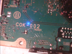
At top side you have the components (and no solders), also is printed in withe the board name/serial, other info for "jumpers" or things like that
And at bottom side you have all the solder points (and no components)
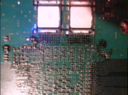
In the PS3 motherboard there are components soldered at both sides, also the name/serial of the motherboard sometimes is printed at both sides too
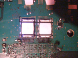
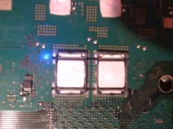
In this case the rule we should follow is to focus in which side is located CELL/RSX, thats top side
Additionally, at bottom side are located all the "testpoints" intended to connect the motherboard with a jig-pin-machine at factory to program it (some of this testpoints are used to solder the teensy flasher btw)
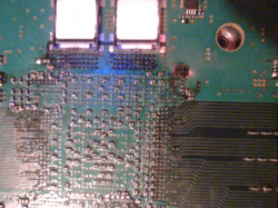
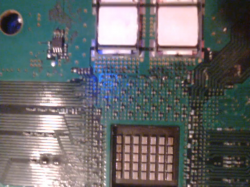
Yep, some people mentioned it before in the thread, that internal layers of metalic materials gets burned at he corners, is a sign that was weared out2, - I see some discoloration on the tokens'. Maybe that is a sign of the problem, or that is how they look like all the time?
Last edited:
")