The theory is...
The tristate is a pin of the southbridge, by "grounding" it all the other input/output pins of the southbridge enters is a "disabled" state (also known as "the third state"... or tristate)
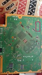
The flash is accessed by other components of the motherboard throught southbridge (it works as an intermediary)
What you want to do is to access the flash contents by using additional hardware (the flasher)... and at the same time you want to power up the motherboard (to power up the flash)
The problem is the data signals from the external flasher are going to have interferences with the other data signals of the motherboard that are trying to access the flash chip
So the solution is to "disable" the southbridge with the tristate pin, this way the flash chip is "isolated" and your external flasher can access to it without interferences
Actually, with the tristate pin you are also disabling access to hdd, usb, lan, wifi, etc, etc, etc... technically you have all the "peripherals" disabled so you have half of the motherboard components "disconnected" from the circuit
Ok... back to the point...

It seems the southbridge of the first PS3 superslim models is exactly the same than all the PS3 Slims, is named
CXD9963GB
https://www.psdevwiki.com/ps3/South_Bridge#Chipnumbers_.40_SKU.27s
https://www.psdevwiki.com/ps3/CXD9963GB
Sadly there is not a table in wiki with the pinout of it
In wiki there is this photo where can be seen the pads under the southbridge (this is usefull to try to imagine where are connected... and to verify it with a multimeter)
https://www.psdevwiki.com/ps3/File:CXD9963GB-desoldered-form-JSD001.jpg
https://www.psdevwiki.com/ps3/File:CXD9963GB-SB-GRID-bw-chipview.png
And this posts from littlebalup where he was looking at it... because someone "destroyed" the tristate pad with a solder iron, so they was trying to find an alternative point to solder on it... and while doing that they had to "follow the copper trace" to an intermediate "hole" in the motherboard (also known as "via") where the trace goes to the other side of the motherboard
That "via" of the photo seems to match with the other photo of wiki (where the southbridge was removed)... and it seems to be connected to the southbridge pin
U2
https://www.psx-place.com/threads/ps3-brick-tristate-point-fell-with-solder.21326/#post-145203
https://prnt.sc/lggnrs
Is very hard to verify all this by yourself (and for everyone), to be completly sure is needed to "follow the traces" in different PS3 motherboards, and are needed photos of the traces under the southbridges (so is needed to remove them)
But sometimes this kind of things can be identifyed with lot of patience by looking at the photos... we are lucky there is one photo in wiki with the southbridge removed
And it looks littlebalup took his time in looking at this in the best way posible, and it seems he was looking at it time ago... so yeah the chances for him to be right are high
")
You can try to review what he is saying by looking at the photos and your motherboard, but most probably at the end is going to be mostly a matter of trying it... or not trying it
I guess you are not going to find a relliable proof (neither me) to know if what he is saying is right or wrong before trying it because we dont have enought info