PS3 Reball ps3 Cell/RSX

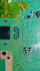
If you don't see any caps shorted on bottom of lan ic nothing to worry, probably power is enabled when system boot is passed, on an specific phase.
d636996c0a4d8b75317e990d9bdf3167.jpg

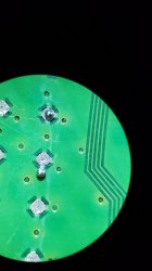
Remember that I asked you for a non working ethernet port? I tried chaging the controller twice, and no luck. There wasn't any short under either. It was wierd. Then, I test the obvious part, the port wasn't giving me continuity using an ethernet cable, but I thought, this is only a port that conduces signals by just doing a mechanical contact.. boy, how wrong I was hahaha.

The internals of that ethernet port are like this:

UkzCsl0.png


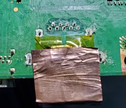
Surely something happened in the inside, and after the replacement it worked like a charm. I used a copper sheet to protect the replacement that I needed to extract and a heatgun. With the solder is a pain in the ass, so with this method is easier and you can remove almost everything ^^
 

Attachments

  • 20210915_131438.jpg
    20210915_131438.jpg
    1.5 MB · Views: 91
  • 20210915_122810~01.jpg
    20210915_122810~01.jpg
    1 MB · Views: 93
This often happened in 2002 with kind of POE network here in my country. Like in 3 months change of network PCI adapter was a must. It can happen over voltage /missing earth to gnd in house electrical circuit protection (yellow+green wire)
 
Something came today in my mind this morning (I don't smoke bad stuff),
A way to get ic soldering on to board with less heat stress.
Instead soldering balls to ic, I've soldered to motherboard.
Pick up tool for balls and working under microscope is more way easier than I thought.
5371de6793e50efd2dcfff1ec2862273.jpg
e4aec3490151462251d2d5da73accf6c.jpg
a5a82a5dac77fbe4f60c9d91e57b0734.jpg
604492e7a45c383814b4717e959c51fd.jpg
b56007619e6deebe31e78d610ab4e04c.jpg
Video with pick up balls tool
http://s.go.ro/eynz1k8m
And final test
http://s.go.ro/ytklg6xy
Parts to modify syringe came from one ciss printer set (bought cheap and never worked, always painted my hands) and adapted to suction pump for ic.
 
Last edited:
Hey @vyktormvmpay25 @sandungas @RIP-Felix have you ever wonder what could happen if you use smaller bgas on both processors? It would overheat due high current and destroy them? I was thinking in minimize the distance between both processors and the mobo, but this could cause a decreasing in cooling performance, I don't know. What do you think? My idea is to use the bgas the least possible, so the time current needs to move through the bgas is the minimum, also creating (huh..) a more stable complete structure of the whole bga map. I mean, if there're least bga volume, it decreases the chances of getting a deformation/degradation/cracks?

By reading a little, I only found recommendations for bga design/installation (not signs of electrical current rule anywhere). By the number of pads=increase the number of bga size. According to a table, more than 1100 pads means you have to use 1.0mm bgas, CELL has 1320..

https://www.xilinx.com/support/documentation/user_guides/ug1099-bga-device-design-rules.pdf

I'm gonna try it anyways lol.
 
I've heard of people recommending 0.55mm instead of the 0.6mm balls for use with direct heat stencils. That way it comes away easier.

I only tried the direct heat stencil method once, with 0.6mm balls. It glued the stencil to the chip and delaminated when trying to remove it! I abandoned the direct heat stencil idea after that colossal failure, but I think like all the other BGA techniques there are tricks I didn't know. In that video you posted the guy added flux to the top of the stencil a few times. I think that prevents the flux from drying out and gluing down. He may have used smaller balls too...IDK, I don't speak much Spanish (or was it portugese?).

I have been thinking I need to revisit balling a chip again. Its been a huge barrier and chalenge. The quality of my other soldering/modding adventures has improved immensely, tho. So too has my understanding of electronics and EE. And that was one of my goals with diving deep into PS3 repairs. At this point reballing has become my white whale...an elusive obsession. A vendetta really!
 
I was thinking in even smaller bgas (0.35) or so. Hmm, what video you say? I also saw people using smaller bgas for the size of the stencil's holes, so that could be a hide truth. I don't think the main issue here could be the bga placement, but the reliability of the fix itself. That's where my intentions are, but like I said, I don't know.

And of course, reworking a heavy pcb like a PS3's mobo is one of the hardest things in electronic (same as micro processors like the ones from cellphones). You need a really good hand to achieve a really good result, and that's where the processors health/maximum life span comes to play, and another list of etcs..

I am too hyped for rework, don't know why. Maybe because is something that not so much people do? Or because of these damn YLOD? One thing is true, since my first PS3 (it died of delidding, not bgas or tokins), the first thing that came to me on youtube was "reballing". I guess that's what it reunite all of us.
 
About small balls may work I think with one condition that board and ic must be perfectly straight. After clear pcb and ic, placing ic and pressing gently onto 2 corners (some ic aren't straight, I have tested many). Just looking between pcb and ic you can view space between them and take decisions. I do not personally think about doing small, that small cap is 0.3mm and in most cases I see that ic is close to them. Is still good idea to bring ic closer to pcb, looking to WiFi board there is no space between, but there is one condition under Wi-Fi. That space between points is far for creating any short between points, so if ic is going down when liquid it may push alloy down so much and possibly to create short on small space as 06 mm.
For my stupid idea of creating an universal jig test board taking time.
RIP-Felix if you find any cheaper preheater of 500 w or any heat resistance you can create your own dual heat rework station. Why do you think I've created that dual heat controller, to replace one very expensive tool that is out of production
https://uk.farnell.com/martin-smt/minioven-04-s/oven-mini-500w-230v-bga-reballer/dp/2352900
I did not had money for it at that time. But I've copied power of that and 500 it's just enough for pcb and ic.An example to one preheater

https://m.banggood.com/GORDAK-853-H...ncy=RON&cur_warehouse=CN&createTmp=1&ID=47757

I will try to explain why my stencil is not wrapped when I'm soldering balls direct to ic with direct heat stencil. Even botakompong have that question why I don't get wrapped.
This must be understand, also I need to remember to add good results for all ps3 motherboard test to working cpu and rsx resistance values.
Also need to share way to remove nec caps without having to use to much heat.
 
I've heard of people recommending 0.55mm instead of the 0.6mm balls for use with direct heat stencils. That way it comes away easier.

I only tried the direct heat stencil method once, with 0.6mm balls. It glued the stencil to the chip and delaminated when trying to remove it! I abandoned the direct heat stencil idea after that colossal failure, but I think like all the other BGA techniques there are tricks I didn't know. In that video you posted the guy added flux to the top of the stencil a few times. I think that prevents the flux from drying out and gluing down. He may have used smaller balls too...IDK, I don't speak much Spanish (or was it portugese?).

I have been thinking I need to revisit balling a chip again. Its been a huge barrier and chalenge. The quality of my other soldering/modding adventures has improved immensely, tho. So too has my understanding of electronics and EE. And that was one of my goals with diving deep into PS3 repairs. At this point reballing has become my white whale...an elusive obsession. A vendetta really!

It's fascinating how many ways there are to do it. I have learned that the stencils that came with my blue jig can only take 0.55 balls despite the marking that it 's for 0.6 mm lol. But those are still the easiest in my opinion. I have direct heat ones too and I actually use them for 0.6 mm (they happen to be accurate) , but I still only use the stencil for placing the pattern and then take it off before applying heat. A few rogue balls will always roll, but you can stop and correct it. I guess @vyktormvmpay25 is doing it differently. So you really need to test out different methods and develop your own technique. I can only say that 0.55 and 0.6 balls both work just fine (I've used both).

Btw Chipquik (the company) is calling them Solder Spheres now . A more professional name perhaps ? :D
 
Last edited:
looking to WiFi board there is no space between, but there is one condition under Wi-Fi. That space between points is far for creating any short between points, so if ic is going down when liquid it may push alloy down so much and possibly to create short on small space as 06 mm.
This is true, it happened to me a couple of times when I soldered those wifi modules. In that case I used 0.35mm bgas, and when I ended with the heatgun, I noticed that one bga was next to the pcb module (it went out easily and safe), this because I surely didn't put the module so precisly and pcb "moved" to fix that. In this case most of those pads are GND, but talking about RSX/CELL is another story.

And, that's why my idea is to get the "no space" between both processors, the way the wifi module is soldered. That would be something different, eh? :D
 
Yes I got your idea. It will be a pain to place balls in first place, if you want to do this, you need an stencil for 03 or so with pitch of cpu /rsx other wise place one by one will be a PITA.
As example 03 mm balls if dropped on stencil of 06 will get inside holes 2 balls instead of o one.
I do not say isn't possible, but challenge is to high enough even for me.
Just in case you test you have to remove those 4 caps on corners to get space.
 
Last edited:
I've wondered about using solder paste in the 0.6mm stencil. It won't equal the same amount of solder but should make balling easier. If less solder is acceptable, it might work.

I just worry each pad wont get the same amount of solder.
 
...I still only use the stencil for placing the pattern and then take it off before applying heat. A few rogue balls will always roll, but you can stop and correct it. I guess
My hands aren't steady enough. I have to hold my breath to get them to steady enough, then all of a sudden I'll twitch and the adjacent balls will roll together. Then I'll get some to melt and adhere, but by then all the flux has dried and the rest of the balls won't adhere. At that point I'm stuck and I can't add more flux or they will swim! It's sooo tedious!

That fine of work is where my patience wears thin. I probably need a proper workbench, microscope, and monitor setup to really step up my microsoldering game.

Cap kits are Level 1. Flex cables are Level 2. Through hole ICs are level 3. Reballing = boss fight!
 
Last edited:
Actually never did with soldering paste on stencil, I assume if clean well on surface it will create that enough amount to solder, only problem is that stencil have to be on right position and well fixed to that place, while we slide to remove excess .Apart from thickness of stencil 0.3mm I don't have confidence to do it. It may work for that situation where ElGris is looking.
Second test with jsd board went fine, reballed both cpu and rsx in reverse mode. Now the time to set stencil on pcb, time to add balls can take time for both. This time I left stencil on pcb and running on rework station direct like reball profile. Soldering take about 6 minutes to one ic side. Stencil get stick to mobo but can be removed later adding flux and heat until is going out but not to much to melt balls again, think 150 is enough.
Now still thinking how to place stencil and placing balls faster, while creating an protective area not loosing balls on board. Aluminium foil way is taking time.
 
I don't understand. I was using 0.5mm for my wifi modules instead of 0.35. Where the hell I read 0.35??? Anyways, I don't get why the pcb on those modules go so attached to the mobo, instead of the ones used on the CELL from super slims, for example. In 42xx it seems Sony used 0.6 on RSX and 0.5 on CELL, or am I wrong? Still, that CELL isn't flat to the mobo.
 
Pads look way bigger for those 0.5mm I'm using. I guess that's the reason. I don't have problem wasting some time to put those bga by hand. I can even do 100, take a break, some coffee, then another 100, and so on lol
 

Attachments

  • 20211024_185236.jpg
    20211024_185236.jpg
    1 MB · Views: 63
Do you have 076 mm? I put that with hand as well. Add thin layer of flux. It will work faster when pcb is preheated with 120. Don't worry about space left between pcb and WiFi, soldering well is working fine.
 
Just did some quick geometry.
0.6mm balls have a volume of 0.0113mL
0.6x0.3mm stencil wells have a volume of 0.00848mL. And solder paste is usually about 58% metal. So the metal volume would actually be 0.00492mL. Solving for radius that would be 0.2273mm or a diameter of ~0.45mm.
using solder paste in the stencil would be roughly equivalent to 0.45mm balls.
 
Back
Top