This is what i meant, i took one of the images posted above and tunned it a bit
")
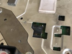
This image could help to see how are connected, and if someone needs it you can use it to draw on top of it, is "clean", i colored the areas of copper --->
https://i.imgur.com/IeTKMbj.jpg
Black = ground
Red = V_IN of the tokins
Orange = V_OUT of the tokins (but also V_IN of CELL/RSX)
As you can see point A and B are connected to each other (and at the other side of the board you have another 2 tokins connected togeter to A and B). Same stuff with C and D
That areas in red and orange colors have the geometry of a rectangle... so if you want to do it simmetrically you can do this with only 1 wire
Note i located the solder points of the wire very close to the VIAS (holes), because that VIAS are what connects one side of the motherboard to the other side of the motherboard... in plain words, im doing it this way because i know that VIAS are the main "river" (are the bottlenecks with the biggest amount of water)... im trying to make a "bypass" in between the bottlenecks
This way is correct too following the same rules i mentioned before, because is symmetrical, the amount of "water of the river" is going to be divided in half, in plain words, every wire is going to carry 50% of the water
But remember... you just need to do this bridging
only if you remove all the tokins
And you can do it with only 1 wire (use a thick wire)... but you are free do do it with 2 or 3 and in both sides of the motherboard, is fine... but most probably is pointless and could be counterproductive because all that solder peaks are going to cause interferences as mentioned before
You know... the amount of interferences is going to be smaller if you do it with 1 or 2 wires... but if you do it with a lot of wires is wrong


 ...i guess "all things come to those who wait" lol


 ...yeahhh.